 Jacob Lewallen
Happy Monday everybody, hope you’re ready for another update! Things were fairly quiet this week as Shah was in Washington DC for the National Geographic Society Explorer festival. My focus was on the preparation for scaling up the manufacture of our FieldKit Naturalist boards.
We have two goals on this front. The first is the assembly of a panel of boards using the pick and place machine at the DesignLab and the second is having the capability of sending away for assembled boards from a 3rd party. In order to be ready to send away for a panel of PCBs, a quick design review was necessary.
Design Review
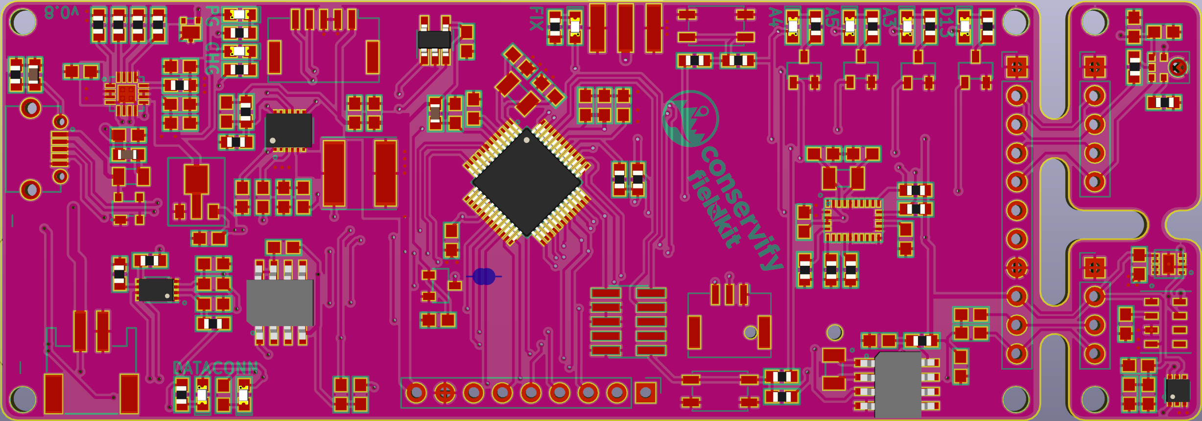
Before:
After:
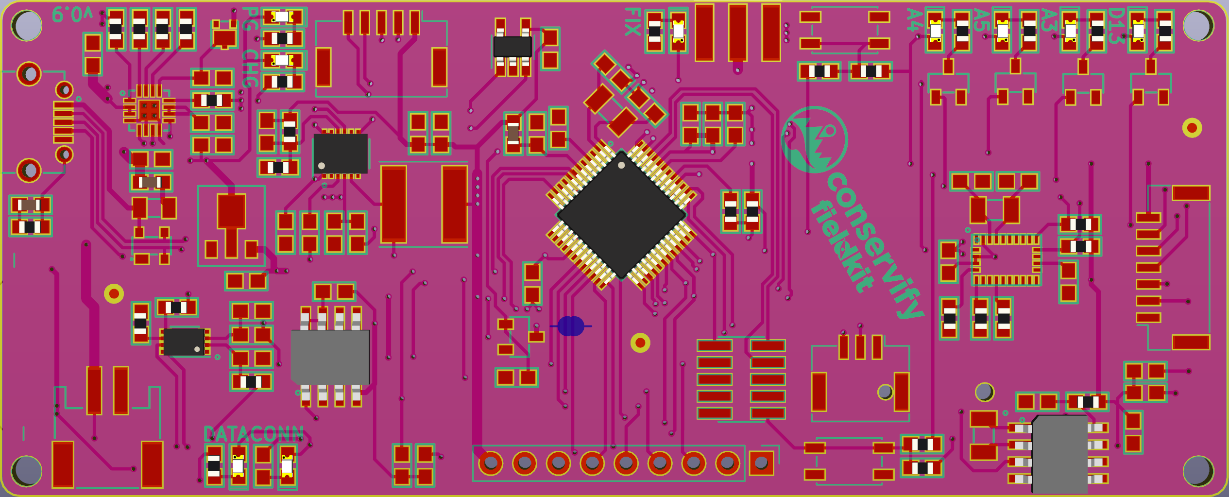
This was fairly straight forward as we have some working prototypes that I hand assembled in our lab and so we have pretty high confidence in our current board design. We did make some changes, though:
- Drop the break-off sensor PCB feature in favor of two separate boards. We had originally intended the break-off design to be useful for STEM settings. Given the relative infrequency of that application when compared to the pre-assembled scenario we opted to just commit to two separate boards.
- We increased the separation between the Micro USB and the SD card. The gap between the two was fairly narrow and we were worried about having thin areas on the enclosure.
- The USB connector was nudged further out so that the board didn’t need to seat right up against the wall of the enclosure.
- Adding fiducials for the pick and place machine. Dan suggested three of them, and that they be as far from other circular features as possible to avoid confusing the CV of the machine.
-
![]()
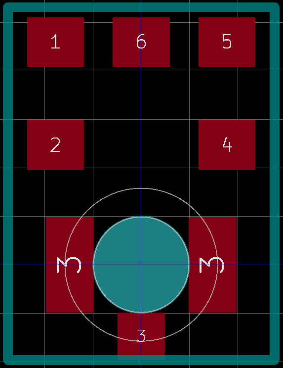
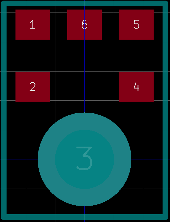
![]() One of our sensors, the SPH0645 MEMS Microphone, has a very strange footprint. The microphone port itself is on the bottom of the chip and so the PCB needs a drill to expose the port. In addition, the chip’s GND is a ring around the port, as you can see to the right. I was worried about solder paste being applied over the top of that drill and potentially sealing off the port. We decided to change the footprint to be more “stencil friendly” by placing some rectangular SMD pads in a way that overlaps the GND ring.
One of our sensors, the SPH0645 MEMS Microphone, has a very strange footprint. The microphone port itself is on the bottom of the chip and so the PCB needs a drill to expose the port. In addition, the chip’s GND is a ring around the port, as you can see to the right. I was worried about solder paste being applied over the top of that drill and potentially sealing off the port. We decided to change the footprint to be more “stencil friendly” by placing some rectangular SMD pads in a way that overlaps the GND ring. - Ensure we have as few through hole components as possible. These greatly increase the cost of assembly. Thankfully this board doesn’t have any of those.
- I asked Dan about the possibility of moving to a 4-layer board and he insisted we stay with 2-layer as long as possible due to the extra cost of more layers.
- Another optimization he suggested, specifically for future boards, is using resistor arrays when possible.
 One of our sensors, the SPH0645 MEMS Microphone, has a very strange footprint. The microphone port itself is on the bottom of the chip and so the PCB needs a drill to expose the port. In addition, the chip’s GND is a ring around the port, as you can see to the right. I was worried about solder paste being applied over the top of that drill and potentially sealing off the port. We decided to change the footprint to be more “stencil friendly” by placing some rectangular SMD pads in a way that overlaps the GND ring.
 BOM Preparation
In ramping up for the pick and place we need to begin ordering pick and place friendly parts - reels and trays. We try and keep all of our BOM information in our schematic files. This means that going into this process each part already had a supplier name and supplier part number, typically from Mouser. Because many assemblers have their own preferred supplier for basic parts like passives, Dan suggested we keep manufacturer details in the schematic as well.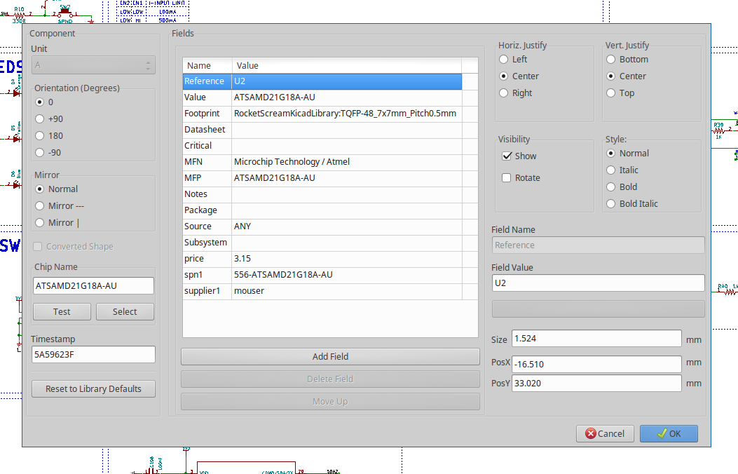
One of the things I love most about Kicad is how scriptable things are. It was easy to export a CSV of the parts and then fill in MFN (Manufacturer Name) and MFP (Manufacturer Part) there and then update the fields in Kicad from that. We also have scripts that go over all of our boards and their parts and look for parts with out-of-sync manufacturer and supplier information. We want the authority to be the schematic, but with several boards keeping the details consistent can be time consuming. Scripts help with that.
Soon, I hope to write a project log about our “grouped spread and place” script. This is a script we use when first starting to layout a PCB. If you’re careful to group your schematic into functional areas using the drawing tools the script will spread the parts out while also gathering related components together on the initially blank canvas, rather than clumping everything together like one giant parts yard sale.
With these things done we plotting the gerber files for the main board and Dan’s going to kick off the back and forth with his preferred assembler!
Discussions
Become a Hackaday.io Member
Create an account to leave a comment. Already have an account? Log In.