 Lefteris Kyriakakis
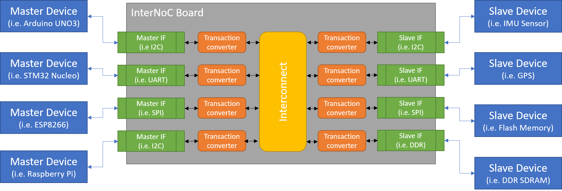
The InterNoC
To eliminate any confusion the following terminologies will be set and used throught the project:
- (AXI) Master / Slave : corresponds to the internal interconnect structure of the FPGA
- Master / Slave device : corresponds to the connected to the device Master/Slave from a system perspective.
- Master / Slave interface: corresponds to the interface used by a master / slave device.
The Architecture
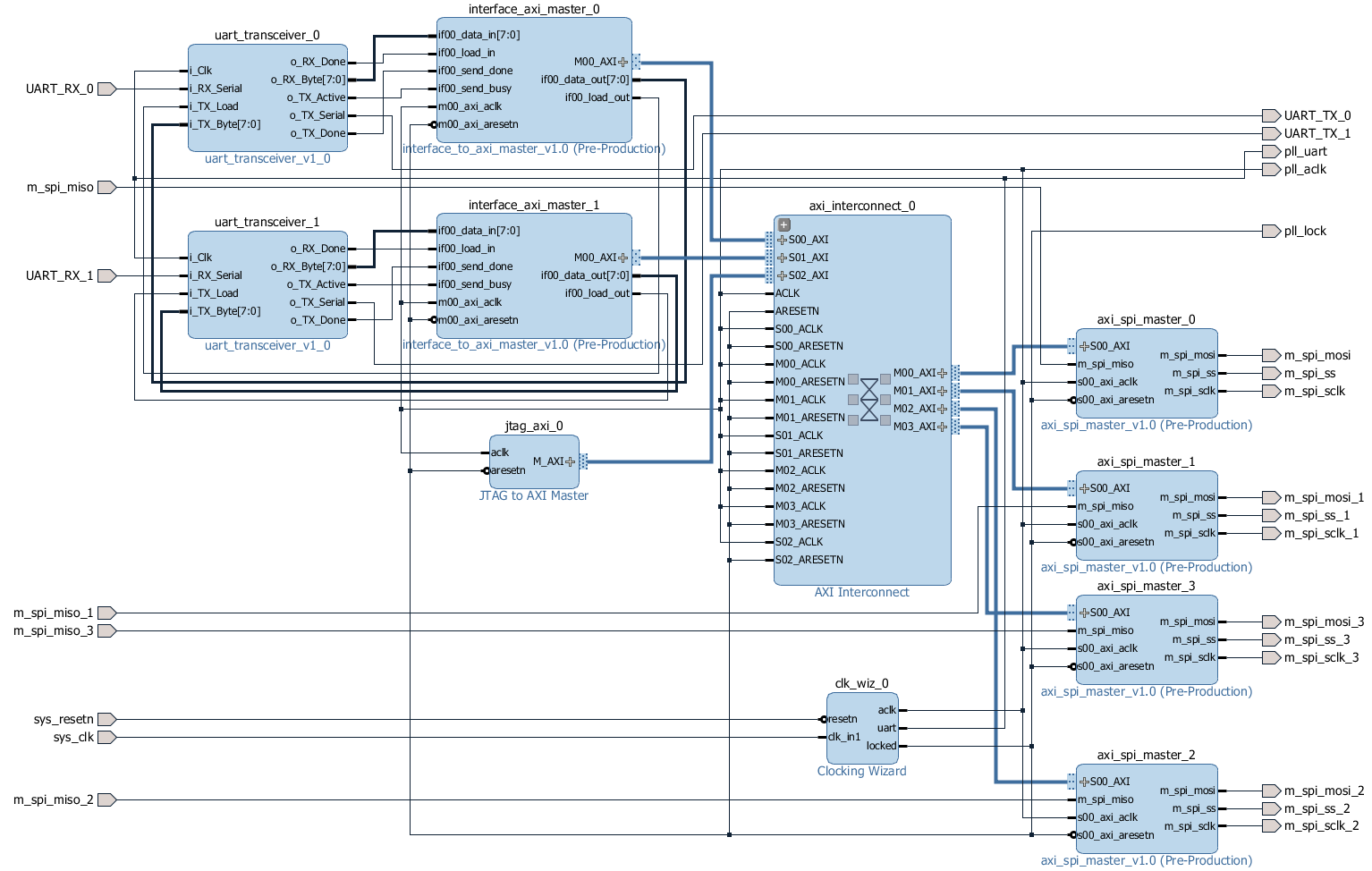
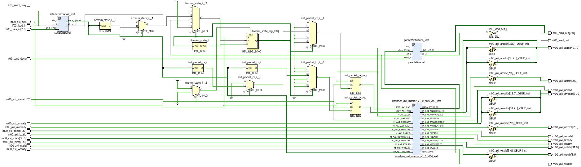
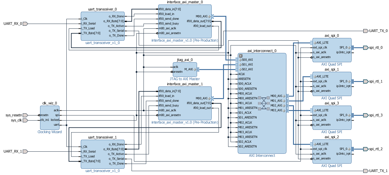
The InterNoC architecture tries to address the N-masters to M-slaves mixed protocol communication issues throughout the physical and application layer by:
- Implementing an abstraction layer between peripheral interfaces and on-chip interconnection accesses.
- On-chip interconnection is managed in the form of AXI memory-mapped master/slave scheme.
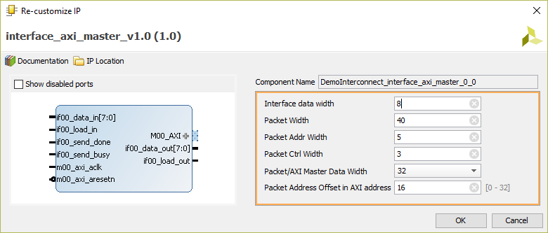
- Conversion IP cores from a peripheral interface to an AXI-MM master/slave
- In the prototype level the on-chip interconnection is managed by a combination of
- AXI interconnect for master-slave accesses
- Shared-memory via use of AXI Mutex for master-master acceses
The Communication
From the user perspective, InterNoC acts like a mixed protocol communication hub of: N(masters) x M(slaves).
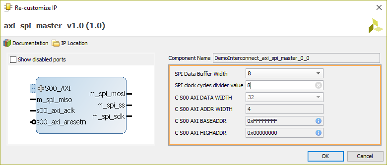
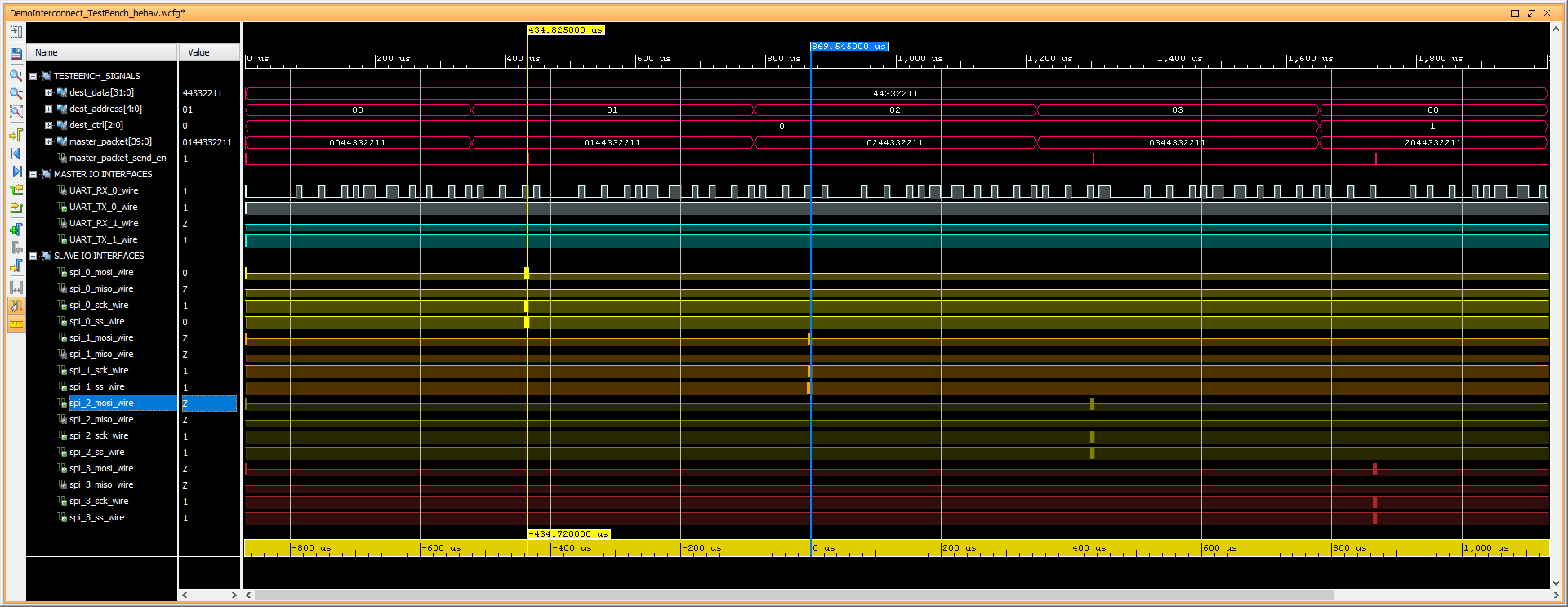
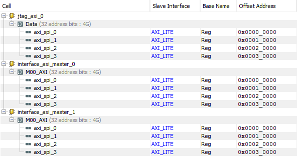
- Communicating through via the NoC will be done in an addressable scheme. Each Master interface port will have a pre-defined address. In order for a user component to communicate to another the Master component will send a packet over the communication link containing the address of the destination component followed by the data. This scheme aims to make the NoC transparent to the user. Master devices will communicate with other connected devices as if they accessed a register address.
- Interfaces will be fixed in the development of the prototype system, i.e. fixed number and placement of SPI, UART, I2C interfaces. Nevertheless, it is in future plans to extend the capabilities discussed and create a fully dynamic, partially re-configurable, mixed communication platform.
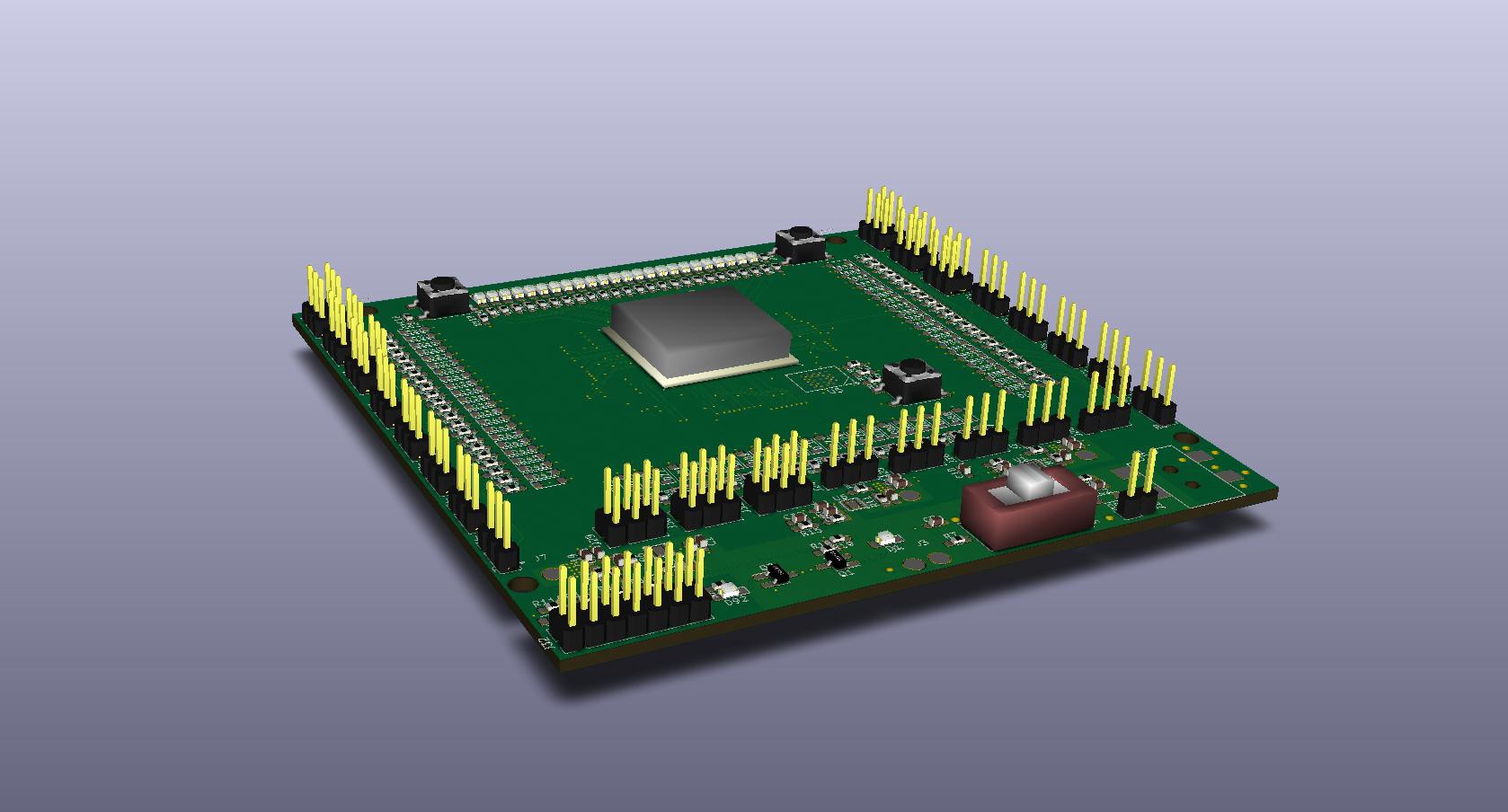
The Hardware
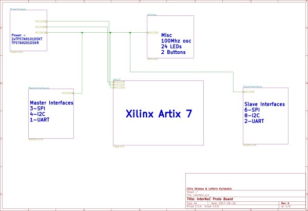
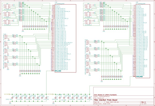
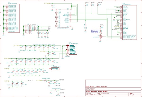
For the current phase of the project the hardware will be comprised of a bare bones artix 7 FPGA implementation along with a set of 2.54mm headers for interfacing common buses (SPI,I2C,UART).
In the future and once we have achieved to have a dynamic platform from the IP side, the solution can be scaled to various applications from low end FPGA solutions with common buses to more advanced automotive CAN bus interfaces to high end PCIe and DDR interfaces.
In the end the ulitmate goal would be to enable a user to inerface an external device with a range of devices from simple I2C sensors to DDR3 memories through the same InterNoC solution.
The Concept


 Wancheng Zhou
 Andrey Ovcharov
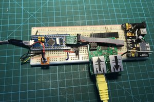
 RT-Thread IoT OS