 Lefteris Kyriakakis
INTRO:
The FPGA Hardware code is managed in the GitHub repository: https://github.com/egk696/InterNoC under the license: GNU General Public License v3.0
CURRENT DEV STATUS:
This is the first dev. log for the InterNoC RTL project. In this log the idea for a mixed protocol is developed and presented on a demo design in Vivado 2016.4. To eliminate any confusion the following terminologies will be used:
- (AXI) Master / Slave : corresponds to the internal interconnect structure of the FPGA
- Master / Slave device : corresponds to the connected to the device Master/Slave from a system perspective.
- Master / Slave interface: corresponds to the interface used by a master / slave device.
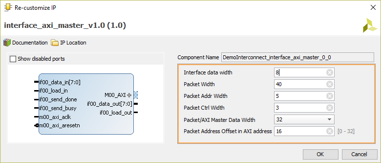
For flexibility and a fixed protocol the decision to use AXILite Master/Slave Bus interfaces was taken. This allows the use of native Xilinx IP cores as well as a unified bus scheme for the FPGA interconnect.
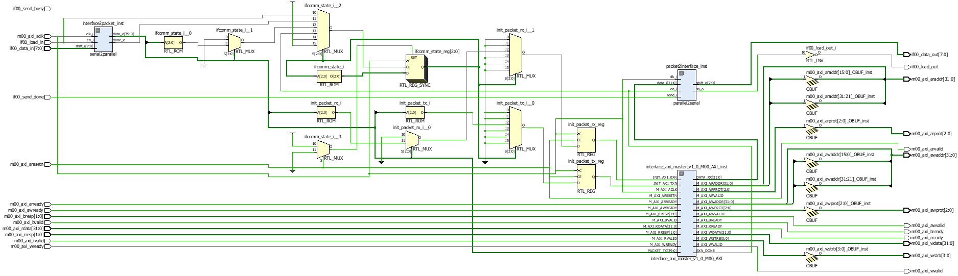
To begin with, the mixed protocol interconnect needed a converter that accepts packets from a master interface and converts it to AXILite master transactions. This component was first developed and is presented below:
The Master-Slave interconnect is based on the Xilinx AXI Interconnect. This choice was made due to its native and easy to implement structure as well as its scalability and flexibility, i.e. it manage multiple clock domains, protocol conversions, arbitration policies and much more.
The final design is build of 3 master interfaces (2 UART and 1 JTAG) all connected to 4 slave interfaces (SPI). For the purposes of prototyping the SPI used is a Xilinx IP Core (https://www.xilinx.com/support/documentation/ip_documentation/axi_quad_spi/v3_2/pg153-axi-quad-spi.pdf) while the UART interface is a personally modified version of the UART components presented in (https://www.nandland.com/vhdl/modules/module-uart-serial-port-rs232.html).
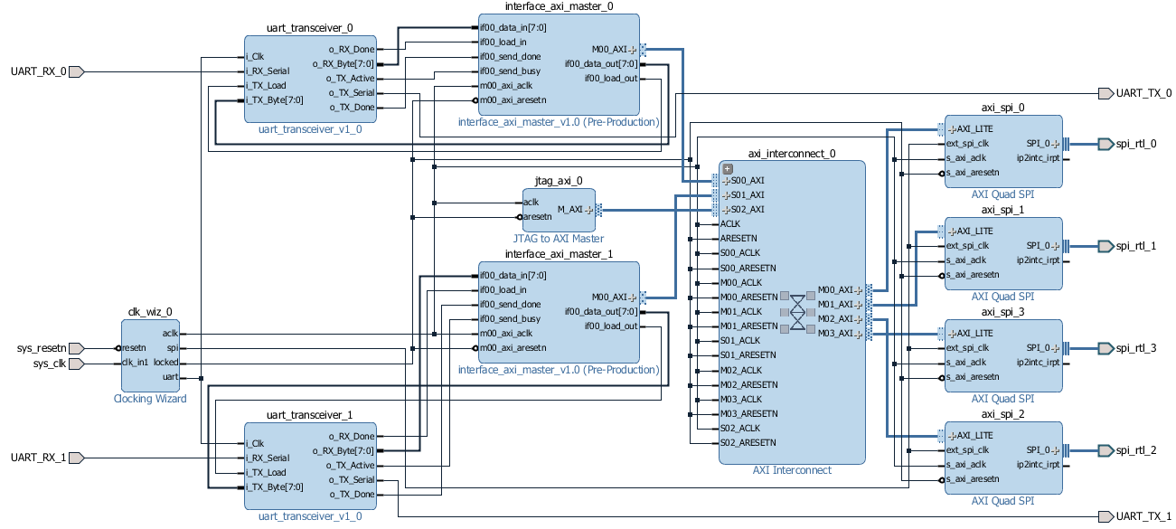
For the current design the baud rate for the UART master interfaces is set at 115200 and SPI slave devices are operating at 25 MHz. In the future solutions will be investigated to support a user configurable baud-rate and clocking frequencies for the interfaces.
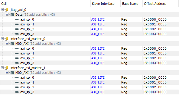
Accessing slaves is done via an embedded in the FPGA address map:
For a master device (i.e. Arduino) to access a slave device, a 40-bit packet must be sent, over the master device's interface (i.e. UART), that follows the following format:
| Control Bits [39:39] | Control Bits [39:37] | Address Bits [36:32] | Data Bits [31:0] |
| Indicates R/W access: "0"=> Write "1" => Read | Indicates Tx/Rx Byte Count: "00" => 1 byte "01" => 2 bytes "10" => 3 bytes "11" => 4 bytes | Support for up to 32 devices i.e. 0x0, 0x1, 0x2, ..., 0x1F | Arbitrary data for slave device |
COMING UP NEXT....
- Master - to - Master communication scheme
- Simulation and Debugging of the demo design
Discussions
Become a Hackaday.io Member
Create an account to leave a comment. Already have an account? Log In.