 Yann Guidon / YGDES
The register set is really the central, critical part of the core, it's the nexus and a physical representation of many logical structures. This explains why I focus so much on this apparently innocuous unit...
Previous posts have examined the register set's low-level structure and here I'm going further by taking the ISA into account.
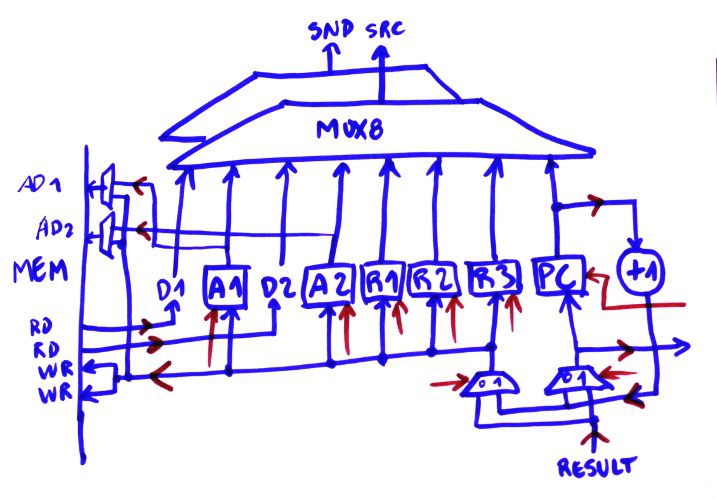
The register map is : D1 A1 D2 A2 R1 R2 R3 PC
- R1, R2 and R3 are "normal registers", implemented the old good way. Nothing to add here.
- PC is "a bit different", since the input has a multiplexer and the output has a direct bypass path to the memory. Oh and it is not an actual latch but an incrementer. Some special cases must be considered...
- A1 and A2 are almost "normal" : they havean extra "read" port/path that goes to the memory's address bus, might be through a MUX.
- D1 and D2 are... quite a mess. Their input is multiplexed because the value can be written from RAM. And it also depends on the configuration of the RAM array : dual port or single port ?
I will now consider the specific case of the VHDL implementation that targets the A3P FPGA family. Reasons include the ample availability of the chips and the ease of VHDL simulation, so I would get working results faster.
The interesting part is the RAM blocks that feature some interesting output latch modes. Only the address ports need to be externally latched and this saves some gates for the data registers. The following drawing summarizes the whole idea :
The wires are usually understood as bytes but here we'll think of them as individual bits because we'll design a first bitslice and replicate it (9 times, including parity).
The bitslice for this part has the following interface signals :
INPUTS:
- of course : SRC and SND addresses (3 bits each)
- Result
- INC output / PC input
- D1
- D2
- SwapSelect (2 signals)
- Write enable for A1, A2, R1, R2, R3, PC
OUTPUTS:
- of course : SND and SRC
- A1
- A2
- PC input
- PC output
- WriteData (post-swap)
it becomes apparent that the register set's structure contains more than latches and MUXes : some signal conditioning is performed in place, in particular the "swap" of PC. The address MUXes could even be performed in place. The corresponding VHDL code is easy to write from there.
An FPGA has different constraints than other technologies and it's a good first step toward full ASIC implementation, particularly with the ProASIC3 family (Actel/Microsemi's A3P, now more than 10 years old but still pretty good for many purposes). So I have tried to make a preliminary layout of one bitslice of the register set (called R7):

The circuit is dominated by MUX2s. There are only 6 DFF but more than 20 MUX2, and soon even more because it's easy to extend the datapath from here. There are also a lot of vertical control lines.
The INC unit has already been designed, and must be routed/laid to form a vertical column of minimal width.
The lower layer (not shown) will contain many decoders to drive the columns : MUX2 controls, DFF enable signals...
The program memory is at the bottom and the dual-ported Data RAM at the left. ALU and SHL at the right, and IN/OUT ports at the top:
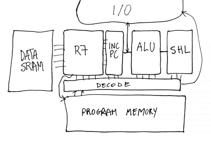
For a FPGA, parity is not necessary at first. However a big missing piece is the debug system, mainly sitting between the program memory and the decoder. A line of MUX might also be sitting between the decoder and R7 to catch the Result, SND and SI8 busses.
Luckily, the PC's incrementer uses quite few gates and can fit in a column of only 1 gate wide :
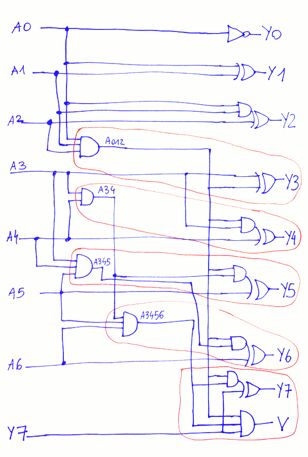
The schematic shows the whole circuit with 13 3-inputs gates only. They can be paired straight-forwardly. I'll have to update the VHDL code.
Another full column of MUX2 selects the result bus' source : ALU, SHL or PORT_IN.
Yet another column of MUX2 selects the source between : register, R/I3 or R/I8.
The whole set is almost square : 15 tiles wide and 16 tiles high, or 240 tiles. Add the ALU and SHL plus some more decoding, that might not reach 500 tiles. This is 1/3 of the A3P060, which leaves quite a lot of room for I/O :-D
Discussions
Become a Hackaday.io Member
Create an account to leave a comment. Already have an account? Log In.
impressive planning and research! it really is amazing how much work goes into creating the instruction set and register organization!
Are you sure? yes | no
Thank you :-)
It's obviously one of the subjects that has motivated me and defined my work for more than 20 years.
I did several napkin projects until dec. 1998 when I joined the #F-CPU project. Years later, I started the #microYasep where I refined my skills and now I'm crystalizing all of this into this recent "minimalist" RISC core. You can see some of the countless thoughts explained in #PDP - Processor Design Principles ;-)
If I can layout the individual gates for FPGA, it's easy to apply this layout for more discrete technologies, inclusing the ones you use ;-) Given that the A3P uses mostly 3-inputs gates, it's easy to make a SOT23-6 version using mostly MUX2 and other simple gates. Would you fancy a kit with an array of maybe 20×20 tiny gates to solder ? :-P
(ok, maybe more in the 24×32 range, but still it's neat)
Are you sure? yes | no
oh that would be interesting! i don't have a problem with soldering that many gates, hehe (see my Mega-one-8-one board!)
Are you sure? yes | no
We'll see how the project evolves :-) I try to maximise general usefulness and once we have a baseline structure (with place & route), the rest is easy. I'm currently testing everything in software (in VHDL) to speed up things :-)
If you have ideas or suggestions, please share :-)
Are you sure? yes | no