 Yann Guidon / YGDES
Yet again another more log about the register set...
Besides the bit latches, the MUX make a significant part of the circuit. One basic block is the MUX4 that clusters 4 bits, 3 MUX2 are required :

(only one bit shown, this circuit is doubled for the 2 read ports)
Nothing fancy here... but it becomes "interesting" when two of these structures are joined:
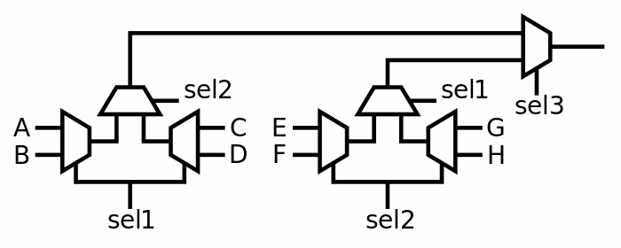
I have applied a "little optimisation" to balance the fanout of the sel1 and sel2 signals (it's the subject of several previous logs and 2 published articles).
I have chosen to not apply further optimisations because it would make the register set even more complex with only negligible benefits.
For 8 bits, the sel3 has a fanout of 8, sel1 and sel2 each have 24 (instead of 16 and 32). Another method would use some sort of pre-decoding of the columns, with one control signal per MUX2, the lateral MUX2 would be driven by signals that are active if B, D, F and H (respectively) are selected. This is an interesting technique for ASIC but not for ProASIC3.
Because of the permutation of sel1 and sel2, the inputs must be re-shuffled. Fortunately the following drawing shows that only two inputs need to be swapped:
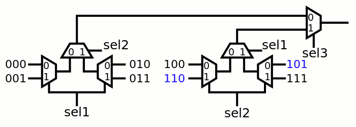
Codes 110 and 101 are numbers 5 and 6, mapped to R2 and R3, which are general-purpose storage and relabelling them is perfectly harmless. In the end, there are 2 MUX signals per bitslice to route over the register array.
If the registers were homogeneous, it would be possible to further swap signals across the array and further reduce the fanout of sel1 and sel2 (sel3 would increase). However this forces more swapping all over the place and routing would be uselessly complicated.
But wait... the codes on the left are not convenient because A1 and A2 should both be on the right of the MUX4 (so they constitute a nice cluster of 4 DFF). Instead of moving the DFF (relative to the first prelayout of the previous log) it's easier to just perform the swap the other way :-) The routing diagram is very simple in the end:
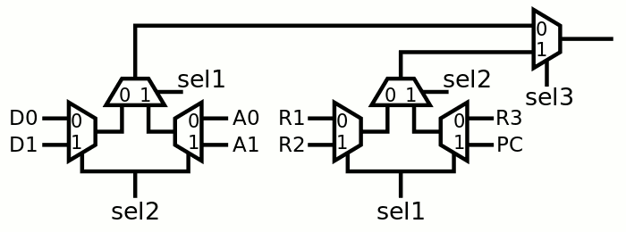
Sel1 and Sel2 are swapped on the left branch, which swaps D1 and A0, without any effort. Neat :-)
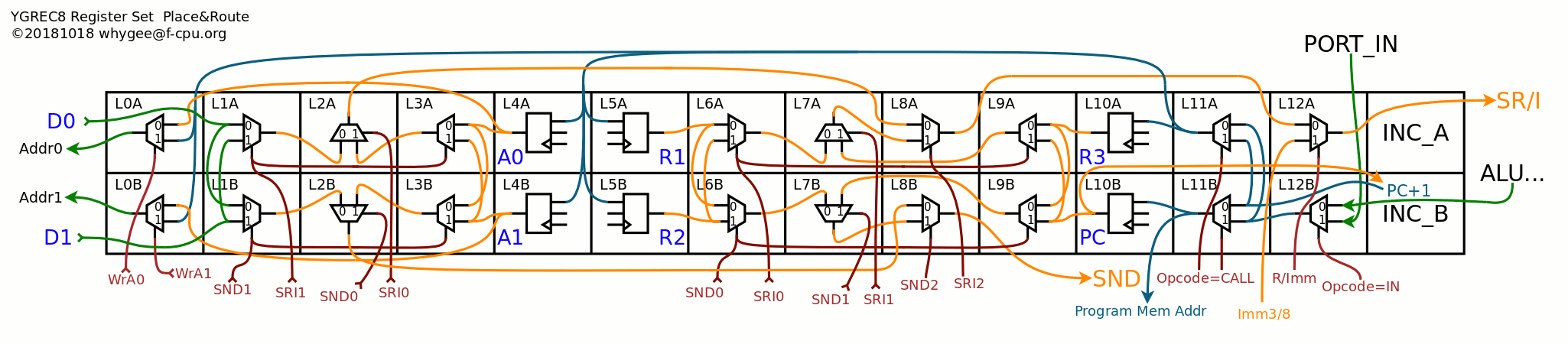
This structure is applied to the more general bitslice:
20181023:
Damnit, I've already found problems with the above diagram :-(
Discussions
Become a Hackaday.io Member
Create an account to leave a comment. Already have an account? Log In.