 Yann Guidon / YGDES
As mentioned in A new assembler panel, I'll soon (hopefully) get a bunch of 4PDT interlocked buttons !
I have already assigned their function but how will I make them work ? Electrically, I only want to have switches, eventually some diodes, and I would love to have the panel use the least power possible, which means ideally no relay. I hope that the panel can be reused for other technologies with the least amount of changes.
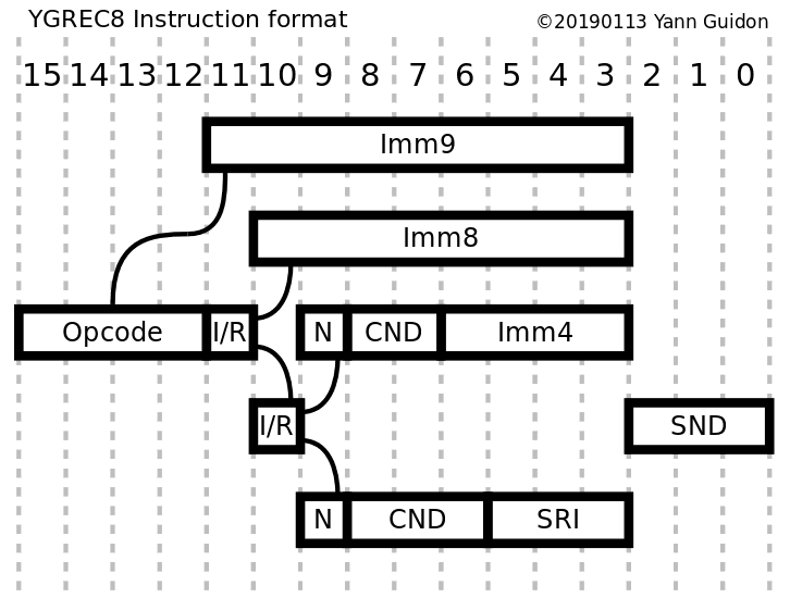
The critical information is contained in these 2 diagrams :
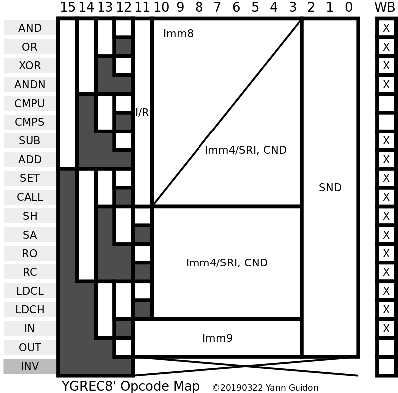 |  |
Already we can see 2 fields that are (almost) fixed :
- The SND field uses 3 bits and a row of 8 buttons that can directly encode the binary code. The 4PDT switches are enough to encode the 3 bits easily. The question is settled and the same system will be used for the SRI sub-unit.
- The Opcode field has 19 codes (and as many buttons). Only RC and INV use 4 set bits so the 4PDT has some spare room, that we need indeed !
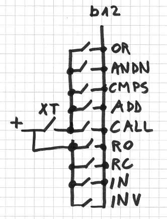
There is no interlocked switch with 19 buttons. The most I have found is 12 so I have chosen to use a pair of 10-buttons rows.
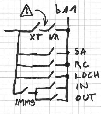
- The upper row contains the SH/SA/RO/RC/LDCL/LDCH/IN/OUT/INV opcodes. That is 9 opcodes. Each 4PDT switch can directly encode the binary value, except bit 15 which is always 1.
- The 10th button of the row is not an opcode but an "escape" button. Let's call it XT, it's an extention that selects the other row (which is the most used anyway) so it's not operated often. The 4PDT switch sets bit 15 to 1 when released (selecting the above opcodes), and otherwise activates the I8/R and Imm8 field.
- The lower row contains the AND/OR/XOR/ANDN/CMPU/CMPS/SUB/ADD/SET/CALL opcodes. Only 3 of the dual-throw switches are needed. The 4th bit remains unused.
How will this work, electrically ?
The panel uses "positive logic" where you implement a bit set to 1 with an electrical contact to an extra signal (usually a bus/rail, such as a positive voltage source). The switches will steer each instruction signal to the common voltage, depending on its encoding.
We can already write some truth equations for the most significant bits of the instruction word :
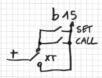
- b15 = ( XT & (SET | CALL))
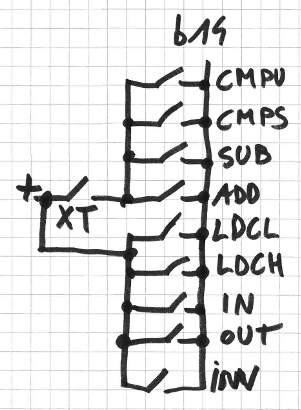
| /XT - b14 = ( XT & (CMPU | CMPS | SUB | ADD))
| (/XT & (LDCL | LDCH | IN | OUT | INV) ) - b13 = ( XT & (XOR | ANDN | SUB | ADD))
| (/XT & (SH | SA | RO | RC | OUT | INV) ) - b12 = ( XT & (OR | ANDN | CMPS | ADD | CALL))
| (/XT & (RO | RC | IN | INV) ) - b11 = ( XT & I8/R)
| (/XT & (SA | RC | LDCH | ( IMM9 & (IN | OUT) ) ) )
As usual the OR operator "|" is implemented by parallel switches, while the AND operator "&" connects switches in series.
The terms contain XT which means the Normally Open side of the XT switch. So XT is a MUX for two sub-buses (b14,b13,b12).
Due to the interlock mechanism, /XT is redundant because it is always off when SH/SA/RO/RC/LDCL/LDCH/IN/OUT/INV opcodes are selected. However the 10 other opcodes are not interlocked and XT must disconnect the affected bits to prevent the other row from interfering.
Updated equations:
- b15 = ( XT & (SET | CALL))
| /XT - b14 = ( XT & (CMPU | CMPS | SUB | ADD))
| LDCL | LDCH | IN | OUT | INV - b13 = ( XT & (XOR | ANDN | SUB | ADD))
| SH | SA | RO | RC | OUT | INV - b12 = ( XT & (OR | ANDN | CMPS | ADD | CALL))
| RO | RC | IN | INV - b11 = ( XT & I8/R )
| SA | RC | LDCH | ( IMM9 & (IN | OUT) )
This is translated into the following diagrams :

The good news is : there is apparently no need for a complex switch for XT because its signal can be shared with several subsignals, thus saving switches...
The bad news is : to prevent certain cases of feedback/bypass (despite the use of independent switches) the output of XT must be guarded with diodes.
However, there are multiple switches per button so the number of diodes is kept low. Here is the census of the usage of SPDT switches per opcode (so far) :
AND: 0
OR: 1
XOR: 1
ANDN: 2
CMPU: 1
CMPS: 2
SUB: 2
ADD: 3
SET: 1
CALL: 2
SH: 1
SA: 2
RO: 2
RC: 3
LDCL: 1
LDCH: 2
IN: 2
OUT: 2
INV: 3
OTOH the XT signal must be split into 5 diode-protected paths.
IN and OUT each use only 2 SPDT switches and 2 are left so each can feed (through a diode) the rotary encoders for IMM8.
XT also can enable the IMM8 encoders through the I8/R switch and 2 diodes. There are 2 encoders :
IMM8_hi = IN | OUT | ( XT & I8/R )
IMM8_lo = IN | OUT | ( XT & I8/R ) | I4/R
Due to the nature of the Hex switches, each output bit must be guarded by a diode as well...
Another interlocked switch selects the format : I4/R, I8/R and REG (they are mutually exclusive).
I8/R is only available in XT mode and otherwise defaults to I4/R mode.
The SRI field (as well as b6) is enabled with
SRI_en = REG & /INV & /IN & /OUT
This uses inverted logic and probably one of the spare/free SPDT of INV/IN/OUT.
Note : I have ordered 8PDT switches for the format selector because I thought it would be useful for actually MUXing the signals but it is not interlocked with XT and others and IN/OUT/INV would not reset the format to IMM8... Diodes seem to be necessary to enable the REG, COND and IMM fields.
The SND field is decoded with the following circuit :

The SRI and CND fieds are identical with some differences :
- The + is not tied directly to the power supply but to a diode-guarded contact of the REG switch
- The CND field is split, depending on the REG switch. The Bit0, Bit1, Bit2 and Bit3 options are enabled by REG (the b3 signal is switched) because otherwise the bit is used for the bit3 of the immediate (in IMM4 and IMM8 mode).
.
.
.
Discussions
Become a Hackaday.io Member
Create an account to leave a comment. Already have an account? Log In.