 Yann Guidon / YGDES
In case you haven't heard the news yet, there is an open source PDK in the making for a 130nm node, and a promise of free, gratis chips !
https://hackaday.com/2020/06/25/creating-a-custom-asic-with-the-first-open-source-pdk/
This is what I had been preparing for, for so many years...
Somehow, I can't access the gates libraries at https://github.com/google/skywater-pdk yet but I can already make a pre-selection of gates I'll use, using data from #VHDL library for gate-level verification and some common sense...
In the slides, one gate struck me :
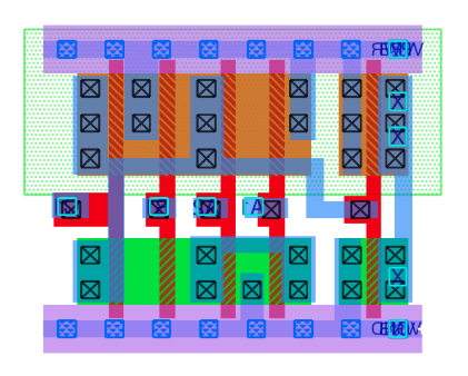
The first reason is : why did they put the amplifier/buffer on the right, when the left side would have been closer and faster... Is it because of a habit ?
Never mind...
The other reason is derived from the discussion of log 103. NAND3 : I have chosen to use gates with not more than 3 pass transistors in series. This limits my choices to these "First order" gates :
- INV / BUFF (x4, x8...)
- NAND2 / NOR2
- NAND3 / NOR3
The above gate, however, is a "second order" gate : there are 2 kinds of logic operations, as it performs /(A and B and (C or D)), and it still fits within the limit of 3 pass in series. There are 4 inputs now... but it's great :-) Now swap the P and N sides and you also get /(A or B or (C and D)).
Drop one input and you even get /(A and (B or C)) as well as /(A or (B and C)). It seems that /((A and B) or (C and D)) as well as /((A or B) and (C or D)) are on the menu, too, and they are welcome precursors to XOR, MUX2 and latches.
Latches are another critical resource to consider... but so far, the gates zoo is expanding and will greatly ease the "NANDification" of the units. This means I'll have to add these new gates to my gates library, after I checked they exist in the SW-PDK.
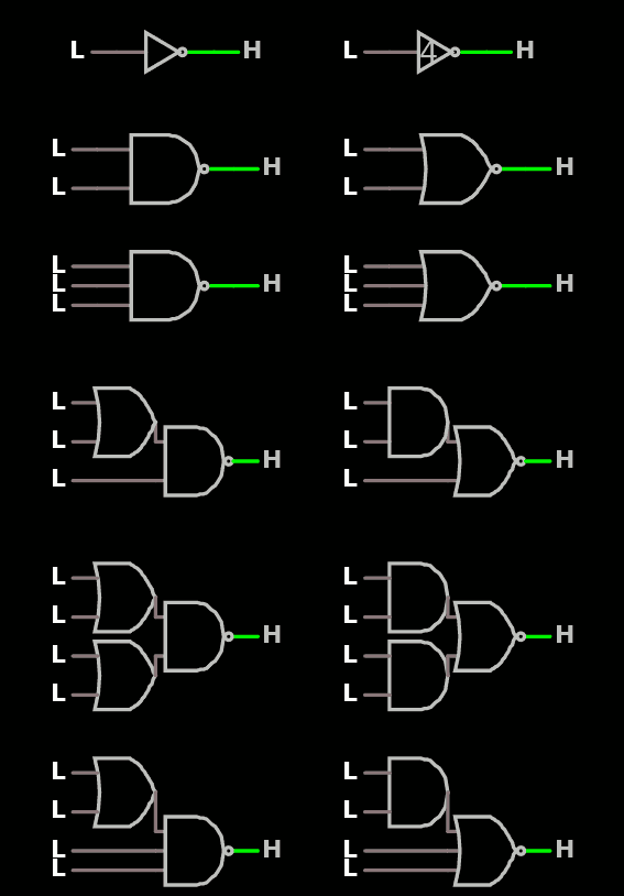
So far the "logic vocabulary" must obey these rules :
- All inputs have a fanin of 1 : the signal drives only one inverter. This greatly simplifies the load estimates when you read a diagram.
- All inputs can have a fanout of 1 : they can drive one single inverter. Logic gates are typically unbuffered. Higher fanouts (usually 4) are managed by ×4 inverting buffers.
- Not more than 3 pass transistors in series between a supply node and a gate (as explained earlier).
This means most gates are inverting. If the fanout increases, an external ×4 buffer will re-invert the signal back to "positive" polarity. This reduces the number of gates to consider. And because NOR2 and NAND2 have only 2 pass transistors to traverse, they could be considered as "a bit faster" or "better fanout" (maybe 2).
The "vocabulary" is listed in this Fasltad window :
There is still a lot of work to do (latches, XOR, MUX...) but it's progressing at last :-) And I can resume the NANDification...
Discussions
Become a Hackaday.io Member
Create an account to leave a comment. Already have an account? Log In.
It is very cool to see this project intersect with the Skywater PDK announcement!
Are you sure? yes | no
it's beyond that ;-)
It feels surreal to be vindicated after two decades of work in this field :-D
Are you sure? yes | no