 Yann Guidon / YGDES
A complete YGREC8 system requires more than the main datapath. The following diagram shows the other necessary blocks :
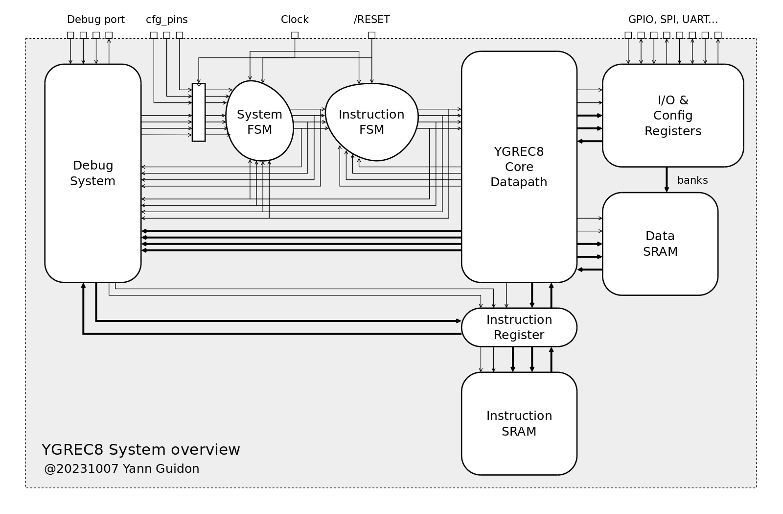
The debug system is essential during development : this is the circuit that lets the developer write and read data inside the system. It can read and/or write :
- the current instruction (read/write)
- the result, SRI and SND (read only)
- the flags (read only)
- the current status of the core (read only)
From there, the developer can inject arbitrary instructions to access the other parts of the system (memory blocks, I/O etc.), dump or modify the state of the system... The debug circuits are totally asynchronous from the main clock, usually significantly slower. The developer must stop the core when inspecting or writing data. It is a bit more intrusive than other debug systems but it is designed to use as few transistors as possible.
The debug circuit has already been started as a standalone circuit but it could be replaced by anything that does the job, such as the Caravel harness used by eFabless (though it is much more complex and uses more real estate, meaning more prone to failure).
The core should be able to work in "standalone" mode, when no host controls the debug circuits. This is usually controlled by the state of some pins during /RESET : the System FSM can wait for a debugger to take control, or the FSM can load external instructions, either passively (as a SPI slave) or actively (by reading from an external SPI Flash chip). If the Y8 system has no internal code storage, you can bootstrap the core by sending 512 bytes through SPI (with an Arduino, RPi or ESP). The System FSM also handles the RESET/LOAD/START/STEP/STOP commands received from the debugger.
The Instruction FSM manages the lower-level details of scheduling the instructions and their details (such as OVL, HLT, LDCx, writes to PC...). This split of the FSM greatly simplifies the design and the modularity. More states are added as more features and corner cases are developed. Meanwhile, the System FSM remains core-agnostic.
The Y8 core does most of the remaining work : decodes instructions, fetches operands, performs operations, write back the results and move things around... It reads instructions from the Instruction Register, which usually transparently interfaces the Instruction SRAM. The instruction can also be read or written by the debug circuit, for inspection, injection as well as for writing a new program or overlay into the Instruction SRAM.
The Data SRAM is a plain memory array. 2 areas of 256 bytes each do the trick but some banking could take place if needed and if the necessary resources are available.
The IO & Config Registers is a user-defined area of 512 bytes that does everything that the rest can't. This is usually where customisation takes place, signals enter or exit the system, default behaviours are configured...
...
Still missing : the interrupt controller. Stay tuned.
Discussions
Become a Hackaday.io Member
Create an account to leave a comment. Already have an account? Log In.