Close
0%
0%

Telemetry System for a Human Powered Vehicle

The development of a modern PCB for 2-way remote situational awareness of a Pedal Prix vehicle used in competitive races.

Similar projects worth following
I have become involved with a company's Pedal Prix team. This 6-24 hour race (seen at http://pedalprix.com.au/) is a horizontal cycling competition that can only be best described as human powered go-karting. As a member of the electrical team I’m partially responsible for the support electronics and telemetry, with the latter being a novelty in the competition. The telemetry allows for a complete situational awareness of the vehicle and the rider from a remote (up to 500m) base station at all times. Vehicle electronics include the lighting, batteries, LCD screen, GPS, RF link, power supply, micro-controller and 3D-printed casing/mount. In the previous two races we have been achieving this in a modular fashion that was consuming significant space and weight. The goal of this project is to incorporate as much of the electronics as possible onto a single PCB.

(Project Shelved - See Log).

First an overview of the entire Pedal Prix telemetry system that the team has developed:

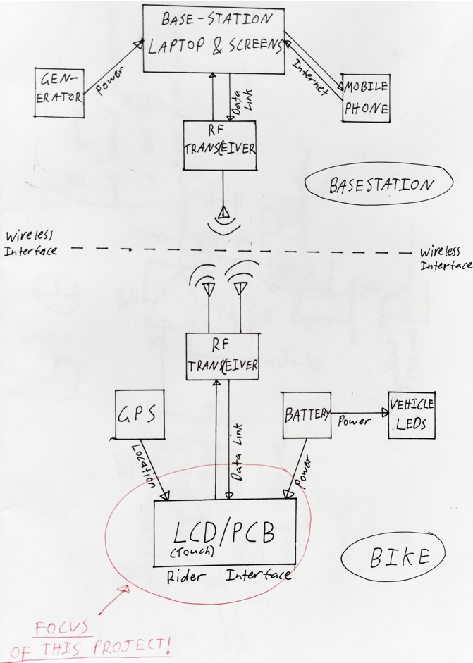
My task and focus is the development of a PCB for the rider/bike side that integrates the other modules together.

The PCB will incorporate the following features:

  • Power supplies
  • Micro-controller
  • Touch screen LCD (the PCB will be mounted to the back of the screen)
  • Complete power measurement (not just voltage)
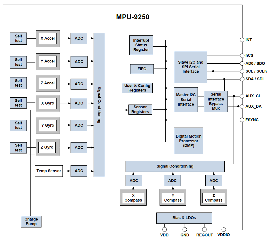
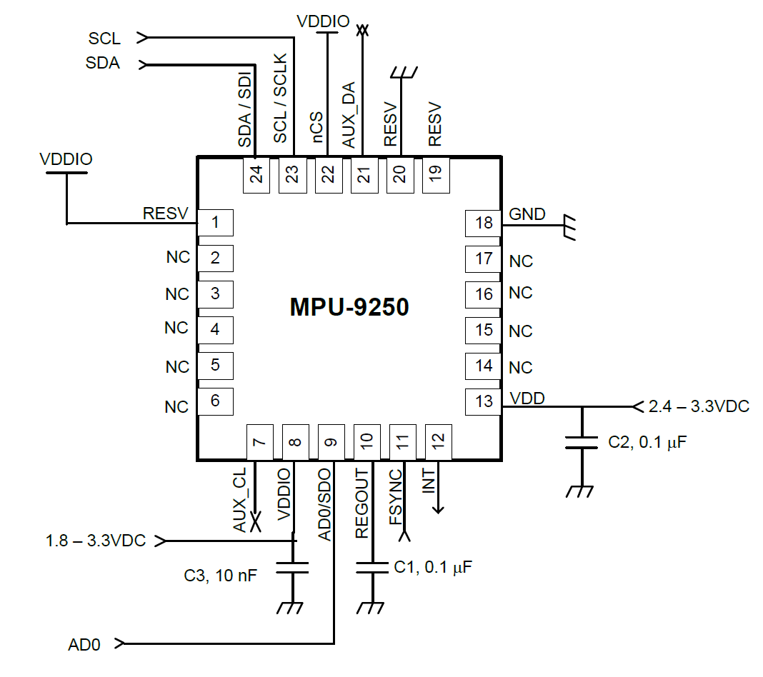
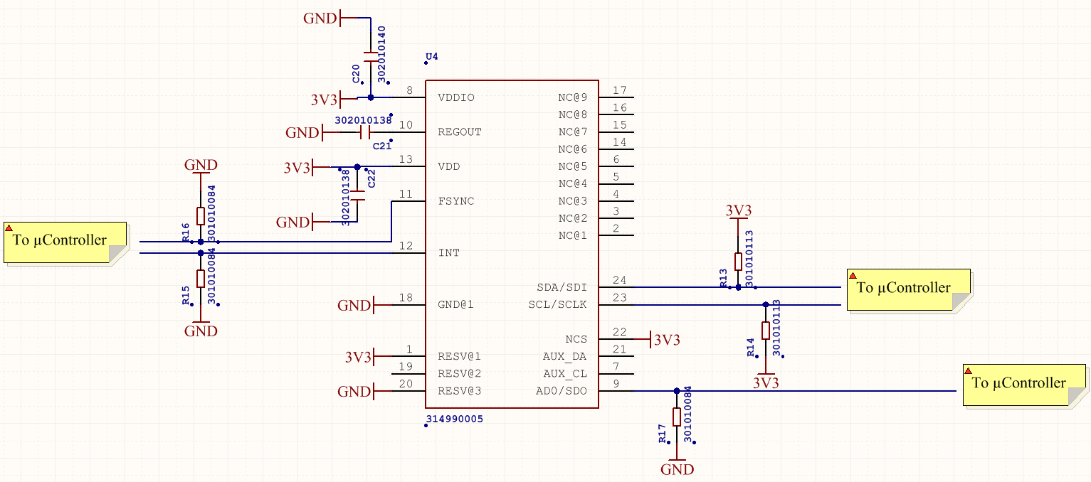
  • A “9-axis” IMU - Allowing for absolute orientation measurement (plus PCB temp!)
  • Power protection features (i.e. polarity and fusing)
  • Plug for wind speed measurement probe (potentially)

Due to the complexity of the RF link (digital multi-node modem) and the location requirement of the GPS antenna, these key functionalities will exist as modules. However, the volume reduction achieved by eliminating the power supply and micro-controller boards will be significant and worth the endeavour!

Project Logs:

  1. Power Measurement
  2. Inertial Measurement Unit
  3. Power Supplies
  4. Project is Shelved for the Foreseeable Future

2017 Pedal Prix Bike Specifications.pdf

2017 Pedal Prix Bike Construction Specifications.

Adobe Portable Document Format - 669.74 kB - 10/19/2017 at 06:30

Preview
Download

RFD900x DataSheet.pdf

RF Transceiver RFD900X Datasheet.

Adobe Portable Document Format - 876.27 kB - 10/19/2017 at 06:26

Preview
Download

GPS VK2828U7G5LF Data Sheet 20150902 GPS.pdf

GPS VK2828U7G5LF Datasheet.

Adobe Portable Document Format - 1.70 MB - 10/19/2017 at 06:27

Preview
Download

Atmega2560.pdf

Atmega2560 µController Datasheet.

Adobe Portable Document Format - 8.41 MB - 10/19/2017 at 05:52

Preview
Download

MPU-9250 IMU.pdf

MPU-9250 Inertial Measurement Unit Datasheet,

Adobe Portable Document Format - 939.94 kB - 10/19/2017 at 06:00

Preview
Download

View all 8 files

  • 1 × Fusion Open Part Library (OPL) A collection of parts that Seeed Studio has the complete EAGLE/Altium footprints for to allow for the quick design and assembly of a prototype PCB. There are certainly some restrictions, but for the most part everything you need is here and guaranteed to be supported by Seeed during the final steps of production. So if you're wondering why some of my component selection seems a bit strange, now you know why. See the OPL here: https://www.seeedstudio.com/opl.html

  • Project is Shelved for the Foreseeable Future

    David Scholten10/25/2017 at 01:19 0 comments

    Due to unexpected circumstances, I will no longer be continuing with the telemetry system on the Pedal Prix bike. As a result, this project will be shelved indefinitely unless some other members of the team decide to post further information as they make progress (unlikely).

    Fortunately, based on the response to the project, it seems not many were interested anyway. A big sorry to those that were though!

  • Power Supplies

    David Scholten10/19/2017 at 11:45 0 comments

    The PCB is powered by a 3 cell Lithium Polymer battery (standard hobby chemistry), which has a maximum voltage of 12.6V and safe minimum of 9.9V. All of the modules and systems (except for the 3.3V IMU) will gladly accept an operating voltage of 5V. However, all the systems that have been selected actually communicate with 3.3V logic (go figure). As a result, the µcontroller must be powered from a 3.3V supply to allow successful integration. To satisfy these requirements, a step-down switching regulator is used to produce the 5V supply (which may see loads of up to 1A), which is then fed into a low-dropout linear regulator to produce the 3.3V supply (that has only light loads <15mA). In this way efficiency and complexity are optimised.

    Linear 3.3V Regulator

    Surprisingly, the Seeed library of parts does not contain many fixed-output 3.3V linear regulators. As a result the regulator selected (LP2985) has the added complexity of an extra two pins for futher functionality (which of course is unused).

    There are some requirements for the output capacitance Equivalent Series Resistance (ESR) to fall within a specified ranges, but almost any ceramic X7R capacitor will do the trick. The design is simple enough and can be seen below:

    The datasheet was even kind enough to offer layout advice, but it’s hardly worth it for a linear regulator.

    Switching Step-Down 5V (5.1V) Regulator

    For the primary power conversion stage that takes care of regulating the battery to 5V, the MP1496 switching regulator was used. This chip is far more involved than the 3.3V linear regulator, but a whole lot more powerful! Below we can see a typical application (for 3.3V):

    The only pins that are important here are 3, 5 & 8, which all relate to the output and its behaviour.

    • Pin 5: The bootstrap pin, which allows for high side switching of the internal transistor. This ultimately allows for a common ground between the input and load.
    • Pin 8: The feedback pin, which allows the output regulation voltage to be set. For our case it was set to about 5.1V
    • Pin 3: The 500kHz switching voltage to be fed to the output filter.

    To select the output inductor, the following formula was followed according to the datasheet:

    The inductor value selected (22µH @ about 2A) for the worst case scenario is a little too low due to Seeed library constraints, which just means the output capacitor had to be sized a little higher (2µF ceramic) according to the 'low ESR approximation formula':

    Which gives a voltage ripple of 34mV, but an additional electrolytic cap ought to help smooth this out. Seen below is the Altium implementation:

    For the actual PCB layout (not yet started), the following datasheet guide will prove very useful in ensuring the correct operation of the device at the 500kHz switching frequency and assist with the positioning of the bypass capacitors, etc. to reduce noise, transmissions, mutual inductance and general high frequency impedance:

    Power Protection Capability

    To protect the PCB from damage or unexpected failures, the following input circuit is used:

    A fuse protects from flame/smoke hazards in the event of a short and two diodes are used to provide reverse polarity protection. D5 blocks the reverse voltage whilst D6 ensures that (in the reverse condition) the impedance of the load is low enough so as to experience a maximum reverse voltage of about 0.5V. Additionally, this input is also connected directly to the 5V and 3.3V rails via a reverse biased low-drop diode (seen in the 5V (D8) and 3.3V (D7) regulator Altium screen shots). These diodes allow energy to flow from those rails to the input in the event that the battery is removed, which avoids reverse biasing the 5V and 3.3V regulators. Without this they may fail on the first power down.

    Coming up next: µcontroller implementation!

  • Inertial Measurement Unit

    David Scholten10/16/2017 at 03:16 0 comments

    During the initial investigation and choosing of the PCB assembly service (Seeed Fusion), I found a “9-axis” all-in-one Inertial Measurement Unit (IMU) that was part of the company’s library of surface mount parts (MPU-9250). This unit, seen below, has a 3-axis gyro, 3-axis accelerometer, “3-axis” compass and temperature sensor. The complexity and functionality of this tiny chip is mind boggling, but it has been made very simple to use thanks to a 100/400kHz I²C interface and a few auxiliary µcontroller I/O connections.

    From a hardware standpoint it is very simple to implement this chip as the datasheet provides more than an adequate explanation of how to wire it up:

    So long as the correct capacitors are used for its bypassing and power requirements (X7R ceramics), there will be no problems!

    The only challenge is to select the pullup resistors for the I²C serial lines, which need to operate at a clock rate of 400kHz. The datasheet lists the input capacitance as “<10pF”, but with the µcontroller connected, the PCB layout and some margin for error, we’ll say the capacitance is 50pF. A 400kHz clock waveform has a total period of 2.5µs and a 1.25µs half period (i.e. one pulse). If we assume the desired rise time to be about a 10th of this, we need a rise time of about 125ns. Let’s make the time constant of the pullup resistor and bus capacitance equal to half of this (62.5ns), which means an 86% rise (i.e. 0V to 2.85V for a 3.3V bus) in 125ns. With a bus capacitance of 50pF and a time constant of 62.5ns, the maximum pullup resistance is 2.5kΩ. For added safety, a resistance of 2kΩ was selected.

    Finally, the schematic is entered into Altium:

  • Power Measurement

    David Scholten10/13/2017 at 09:34 0 comments

    Each Pedal Prix race has a running time of at least 6 hours, which is demanding on the capacity of the battery (that has already been minimised in size to reduce weight). As such, it is almost guaranteed that the battery needs to be replaced at least once during the race. To maximise the usage of each battery it is highly desirable to know the remaining electrical energy at all times during the race. This therefore requires both voltage and current measurement capability on the PCB.

    Voltage Measurement:

    Voltage measurement of the battery is very simple, consisting of a resistive divider and a filtering capacitor. So long as the divider resistance is low compared to the µcontroller input, no current buffer is required. As the battery voltage is “stiff” (i.e. no sag under the expected current draw), the voltage does change transiently. Thus, there is no AC component to the voltage source (battery) and the measured signal can be heavily filtered. Filtering cannot be used when both the source voltage and load current contain AC components (potential for phase differences and a power factor below 1).

    Current Measurement:

    Thus, as the source voltage is effectively pure DC, the measured current signal can also be heavily filtered as the power measurement is now simply the battery voltage multiplied by the average current. However, the current is technically more complex to measure due to shunt requirements.

    A shunt on the positive side of the battery terminals requires a differential amplifier to condition the signal to have a zero point at ground. However, the voltage must be first divided down to protect the Op-Amp that is powered by only a 3.3V rail. This in turn reduces the differential Op-Amp voltage output and increases the gain requirement of a subsequent cascaded Op-Amp stage.

    To correct this over-voltage problem, a shunt is instead used on the return side of the battery. Seen in the image, the 0.1Ohm shunt produces a small voltage that is negative with respect to the rest of the system (Op-Amp included). The Op-Amp chosen for this role should have:

    • A common mode range that extends beyond the rails (i.e. about Vee-0.1V to Vcc+0.1V).
    • Rail-to-Rail operation at the output to allow for a true zero-voltage output for an asymmetrical power supply (i.e. no negative rail available).
    • The ability to function with a small supply voltage (3.3V rail).

    So long as the Op-Amp can achieve these goals (OPA333AIDBVT was chosen) we can simply use an inverting Op-Amp configuration that allows gain relative to the true ground zero-point, but inverts the signal. Effectively, the non-inverting amplifier is a differential amplifier anyway (0V minus the negative signal), so the inversion comes naturally. As an added bonus, low pass filtering can be simply integrated with a single capacitor in parallel with R2 (infinite roll off!). The equation for the entire system at steady state is (i.e. DC component only):

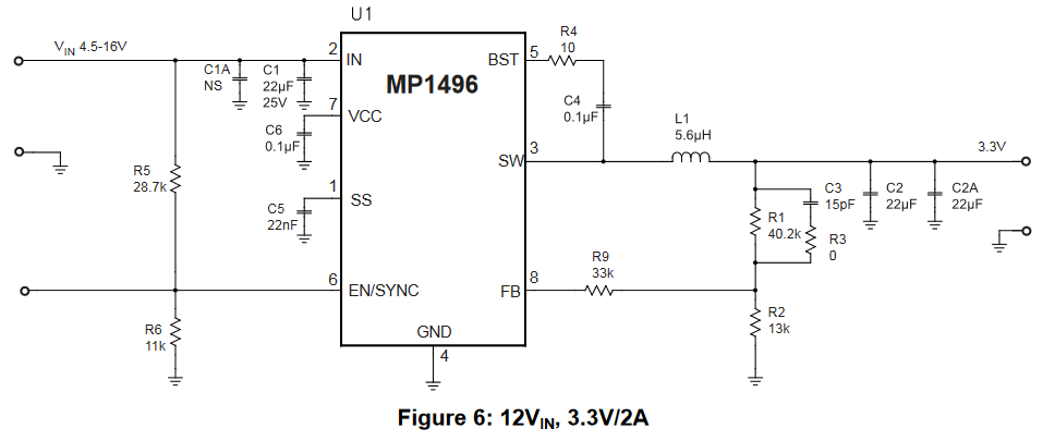
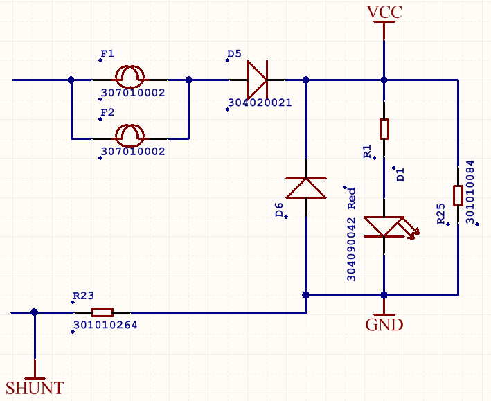
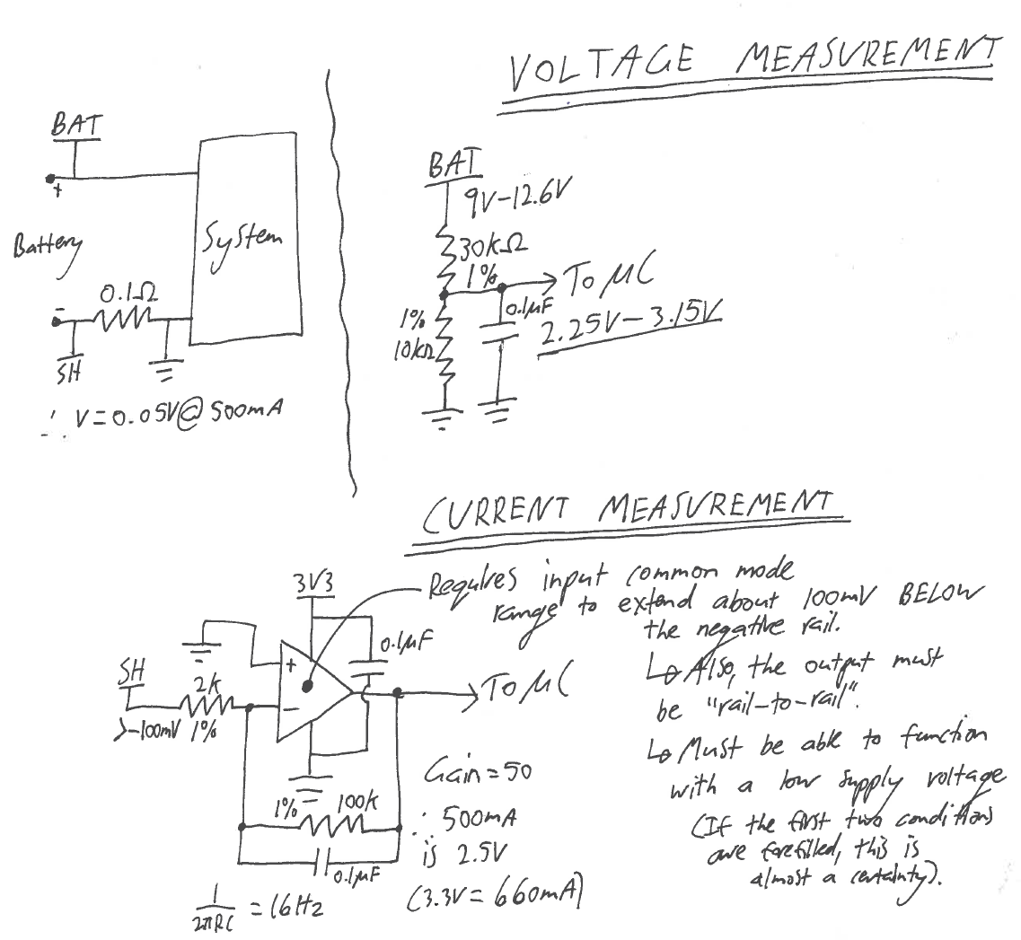
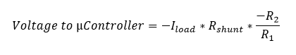
    Where the maximum voltage of 3.3V represents 660mA for the µcontroller in the presented system. It is important to note that the exact resistance of the shunt needs to be known.
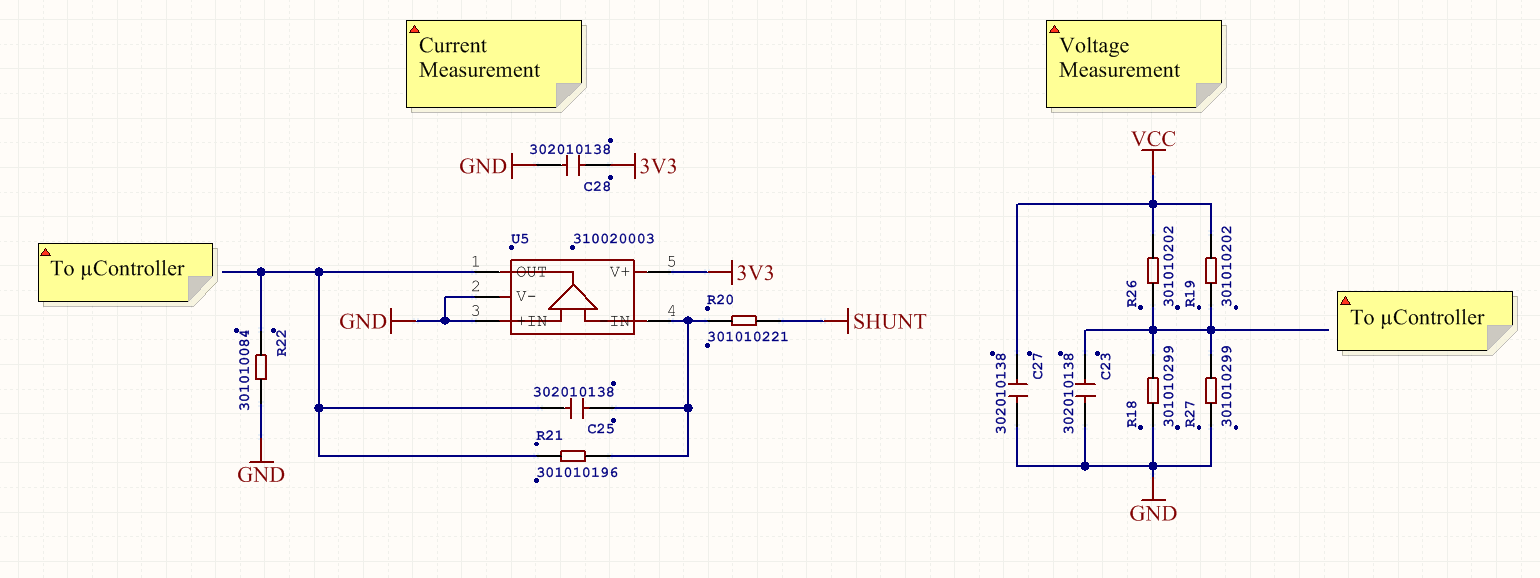
    Finally, here is the Altium 2017 implementation:


    In the end it's nothing more than a basic Op-Amp implementation, but it was fun none-the-less!

View all 4 project logs

Enjoy this project?

Share

Discussions

Similar Projects

Does this project spark your interest?

Become a member to follow this project and never miss any updates