Close
0%
0%

TinyFPGA E-Series

Tiny board with a BIG FPGA. SD card, 64mbit DDR RAM, ECP5 FPGA, 64mbit flash, and micro USB. Do more with up to 45k LUTs.

Similar projects worth following
The TinyFPGA E-Series boards take TinyFPGA boards to the next logical step: more features and BIG FPGAs in a tiny form-factor.

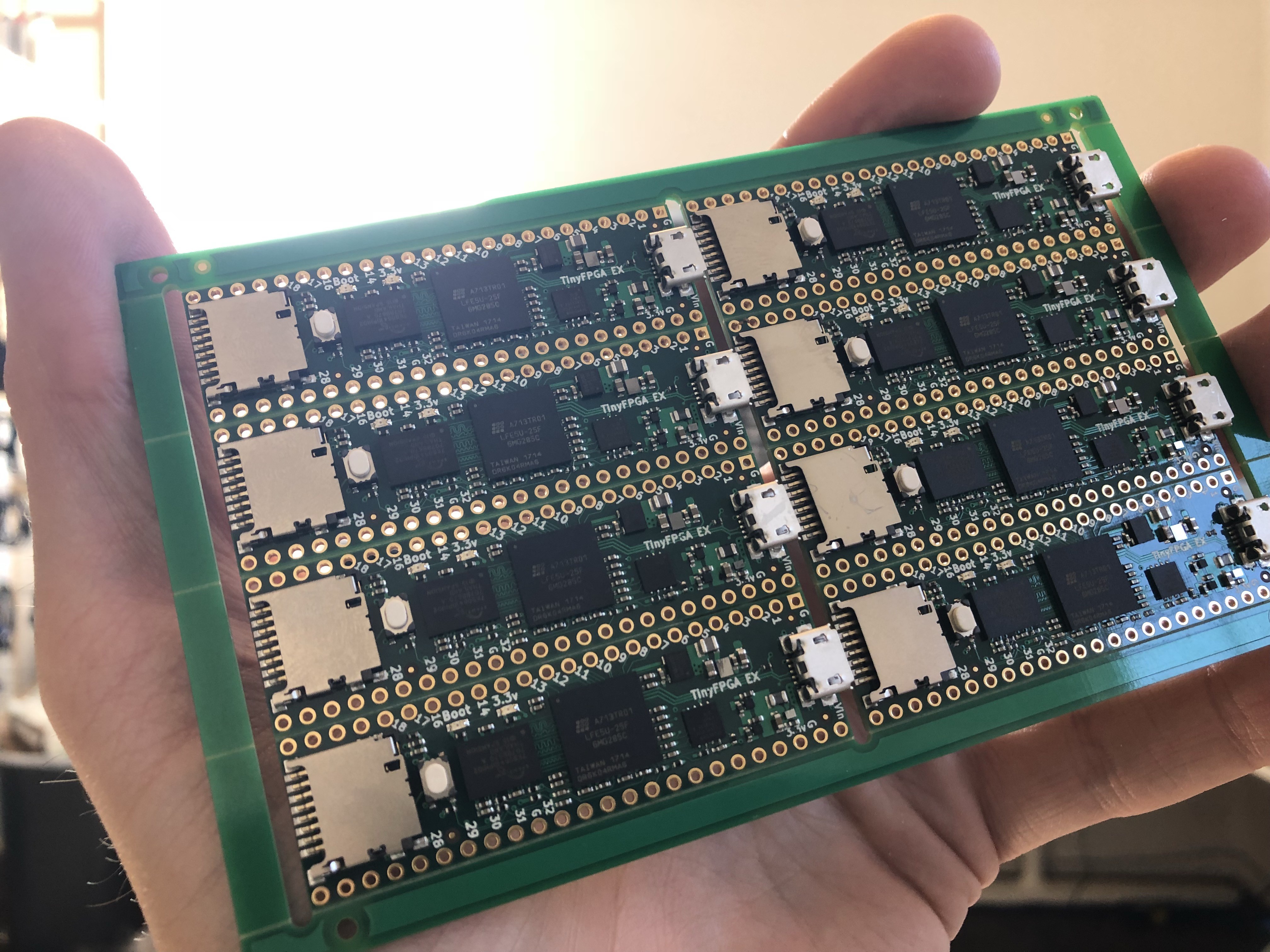
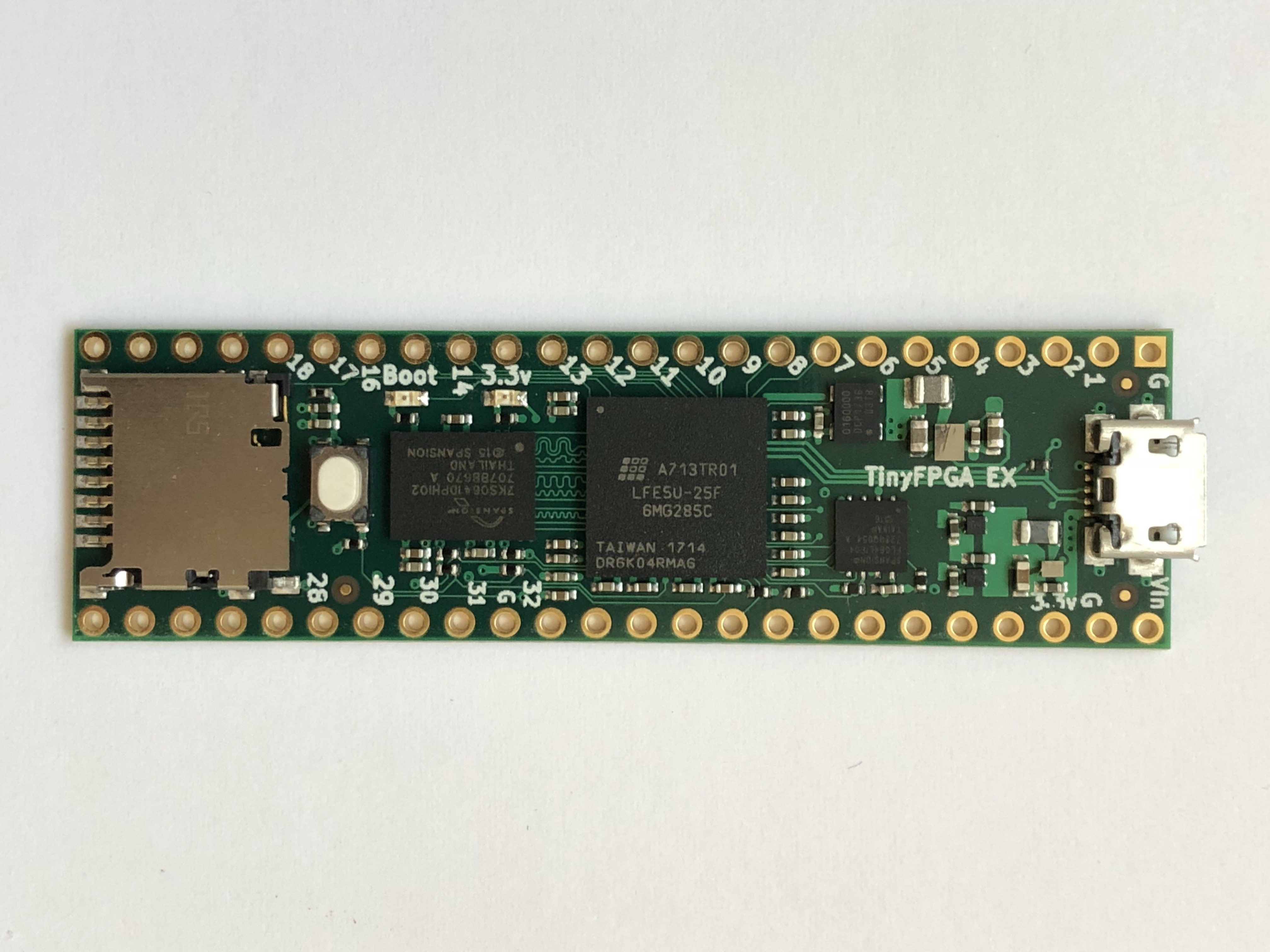
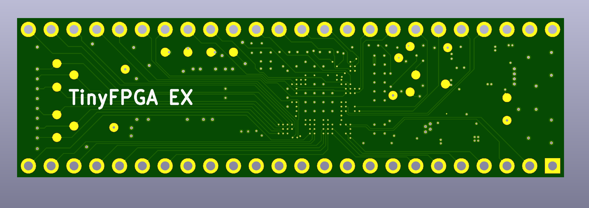
The TinyFPGA E-Series boards take advantage of Lattice Semiconductor's ECP5 FPGAs in a tiny 10x10mm package.  These boards use three different ECP5 FPGAs: 12k LUT, 25k LUT, and 45k LUT devices.  In addition to big FPGAs, they contain a few other features only found in larger boards:

* Micro SD Card Slot
* 64MBit DDR HyperRAM
* 64MBit SPI Flash
* 3.3v switching power supply for IOs
  * 2.5v LDO for FPGA aux rail
  * 1.8v LDO for HyperRAM and associated FPGA IOs
* 1.1v switching power supply for FPGA vcore (up to 3 amps...)
* 16MHz MEMS clock
* Micro USB connector
* 42 GPIOs
* JTAG, SPI, USB test pads on bottom
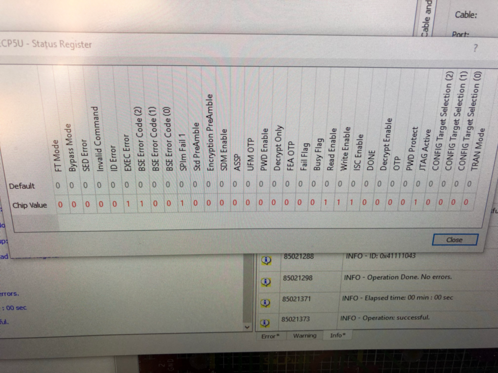
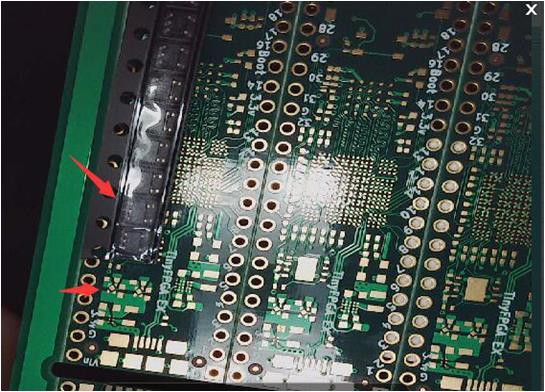
  • Prototypes Arrived!

    Luke Valenty02/10/2018 at 23:11 6 comments

    After months of waiting the TinyFPGA EX prototypes arrived a few days ago!  I was so thrilled to finally try them out that I forgot to write a Hackaday.io post about it.  

    The prototype run was for one panel of 8 boards.

    The first thing I did was check the bare PCBs that were sent alongside the assembled boards.  It looked like there were vias missing.  An inspection with my USB microscope seemed to confirm this.

    I took out my multimeter to check the resistance between various pads and the external pins.  Despite looking like there are missing vias, their is a reliable connection between the pads and their respective pins on the board.  I'm not sure why the vias aren't visible.  Maybe the plating filled in the small holes completely?  

    While I had the bare PCBs under the microscope I took a look at the pads for the power supplies.  The two switching supplies are tiny BGA packages.  The 1.1v supply can supply up to 5 amps of current!  However, the inductor I choose is rated for up to 4.3 amps.

    There are also a couple of linear LDO regulators that have a unique footprint.  They are super tiny.

    We can see that the PCBs very good quality considering the tiny size of the components and traces.  Afterwards I wanted to take a look at the power supplies as assembled on the board.

    Grey surface mount passive in the corner is the inductor for the switching power supply in the center.  The brown components are the input and output capacitors.

    The two switching supplies appear to be assembled properly and the footprints are good.  

    The linear LDOs are each capable of sourcing 300mA of current.  They are used for the HyberRAM and the VCCAUX of the FPGA.  After inspecting various components I broke out a few boards to start the process of bringing up and debugging a new FPGA board.

    Before powering the board on, I wanted to make sure I wasn't going to let out the magic smoke.  I measured the resistance between the ground and various supply pins.  They were all high enough resistance that dangerous shorts were very unlikely.  I was confident enough to apply Vin.

    It worked!  Well, at least the 3.3v switching power supply worked well enough to light up the 3.3v power indicator LED.  I checked voltage levels of all the power rails and they were spot on.  Another good sign.  Next step is to see if the FPGA itself is functional.  To do this I would want to connect the JTAG interface to the Lattice programming cable.  The JTAG test points are on the bottom of the board and I didn't have a test-jig setup yet so I would need to solder some cables to the test points.

    In addition to the JTAG port, the flash SPI interface is also on the bottom.  I connected headers to both of these ports so I could spy on the configuration sequence.  Running a simple ID code read on the Diamond Programmer application I got a sign of life from the FPGA!

    This is a very good sign.  The basic functionality of the FPGA is working.  I discovered I could also read out the status register from the FPGA.

    The status register reported an error.  After reading the Lattice documentation I decoded the message.  It translates into the following English: "I couldn't load a configuration from SPI flash.  The data stored there didn't have a valid preamble."  Very cool.  The ECP5 FPGA can be configured in multiple different ways.  I had setup some pull-up and pull-down resistors in a few pins to tell it to pull its configuration from flash.  It appears to be working!  Now I needed to load a valid bitstream onto the SPI flash.  To do this, I wanted to use my USB bootloader from the TinyFPGA B2 project.  This means I would need to port the bootloader over.

    It was actually a lot easier than I expected.  The FPGA programmed...

    Read more »

  • Always check your BOM...

    Luke Valenty01/11/2018 at 08:27 0 comments

    The E-Series prototype boards were going to assembly at my PCBA house when they discovered a problem.  The linear voltage regulators did not fit on the footprint.  After having a minor heart-attack I looked at the picture they sent and understood what happened.  I had given them the wrong part numbers.  They were off by one letter.  I gave them part numbers for a different physical package.  Thanks to the picture they sent it was easy to remedy.  Always double-check your BOM before manufacture.  This was not a big deal because it's just 16 components and they are very cheap.  But it did delay assembly another week while they source the correct parts.

    On the bright side it was nice to see a picture of the prototype PCBs :)

  • Still waiting for prototypes...

    Luke Valenty12/25/2017 at 07:16 0 comments

    I'm still waiting on the prototype boards!  Currently I'm waiting on getting the ECP5 parts.  This should happen soon.  In the mean-time I'll need to make a pogo-pin test rig and general-purpose testbench for it.

  • Prototypes Ordered

    Luke Valenty11/21/2017 at 07:08 0 comments

    I sent the gerbers and associated files to PCBWay for manufacture and assembly.  The BGA package on the ECP5 FPGA I'm using requires 0.15mm via drills and 4 copper layers to route out all the necessary IOs, grounds, and power rails.  This means it's an advanced PCB process that has much more expensive fixed costs.  I've reviewed the board layout and schematic several times.  It should work.  I think.  It will be very interesting to see what sort of issues pop up.  When I do get the prototypes back in a month (if I'm lucky it will be that fast!), I'll have the following things to checkout in roughly this order:

    • 3.3v switching regulator
    • 1.1v switching regulator
    • 2.5v LDO regulator
    • 1.8v LDO regulator
    • FPGA JTAG
      • I should be able to hook it up to the lattice programming cable and get some signs of life
    • SPI Flash
      • I should be able to read and write the SPI flash using the testpoints
    • FPGA/flash connection
      • I should be able to make a simple LED blinky design to make sure the FPGA can read its configuration from flash.
    • 16MHz MEMs clock
      • I should be able to make a design using the 16MHz clock and it should work
    • USB Bootloader
      • I'll be porting the #TinyFPGA B-Series USB bootloader to the ECP5 FPGA.  I've included a dynamic pull-up resistor on the USB lines so I can make the connect process more reliable.
    • HyperRAM!
      • I'm super excited about the HyperRAM...but it will be a new challenge to develop a robust interface for the HyperRAM since it uses a unique DDR protocol called HyperBus.

    There's plenty of work to do while I'm waiting for the boards.  Beyond getting ready for the initial checkout of the prototype boards, I'll also be designing a pogo-pin test bed for production checkout of all TinyFPGA E-series boards.  The pogo pins will contact each of the IOs as well as all of the power rails and test points on the bottom of the board to access the SD Card interface, JTAG, SPI, PROGRAMN, 1.1v, 1.8v, and 2.5v nets.

    Bottom of the TinyFPGA E-series board with test pads

  • A new TinyFPGA series to fill out the tiny line-up

    Luke Valenty11/18/2017 at 20:50 0 comments

    When I started working on TinyFPGA I was making a simple FPGA board for myself.  That simple board became the #TinyFPGA A-Series.  I chose the MachXO2 for the first board because it was a very simple to use FPGA and it had a very easy to assemble QFN32 package.  It was something I could reliably assemble and reflow myself in my home lab.  I ended up getting it manufactured anyways.  But that package made it cheap and easy for the first prototypes.

    After developing the A-series, I had a desire for more.  A larger FPGA and more features built-in.  I also had more confidence with one project under my belt.  The #TinyFPGA B-Series was a much more complicated board to develop.  It uses an FPGA with a 0.4mm pitch BGA package with 81 balls.  I was able to make it work very reliably with a common PCB manufacturing process so my prototypes were cheap and functional.  I also was able to deliver a lot more features in a tiny package.

    All of the TinyFPGA boards are selling well enough to give me confidence and now I need to refresh my stock.  So I have been ordering new boards and have learned quite a bit from my original manufacturing runs.

    I still want to be able to deliver more options for these tiny FPGA boards.  I think I found a way.  The Lattice ECP5 FPGAs have relatively low power consumption with prices way lower than comparable alternatives.  That's good to know, but the best part is the package size.  They have a package option that is just 10 x 10 mm and is available across the entire range of ECP5 FPGAs.  This means I can develop one board and support multiple FPGA sizes.

    With the ECP5 FPGA and the TinyFPGA E-Series, I think I am pushing the limit of what will work in this form factor with today's technology.  The package size, number of balls on the package, power delivery requirements, and PCB manufacturing technology are all being pushed to the limit at this price point and form-factor.

    Not only will these new TinyFPGA boards feature FPGAs rivaling the size of any hobbyist FPGA board, they will also include 64mbit DDR memory, 64mbit SPI flash,  high-efficiency switching voltage regulators, and a micro-sd card slot in addition to all of the features on the B-series boards.

    It has been quite a challenge designing this board and there are more challenges to come.  The next step in bringing these to market will be getting the prototype boards back and running them through their paces.  If you want to use big FPGAs in a tiny form-factor without breaking the bank, follow this project.  I'll be posting updates as boards come back and development progress is made.

View all 5 project logs

Enjoy this project?

Share

Discussions

SHAOS wrote 09/26/2023 at 20:27 point

Any updates? Thanks!

  Are you sure? yes | no

Clem Morton wrote 04/02/2019 at 05:33 point

Nice!

I have a project planned that might make use of some of your boards. I'm hoping. Depends on how testing goes. Currently i'm waiting for some prototypes to arrive, if I can get them up and running i'll move forward with some next steps. Know of any resources where I can learn about passing i2s audio streams through? Simply from one set of pins to another. The idea is to use one of your boards as essentially a signal router. And place it daughter board style into a larger project. This will allow me to route the i2s audio streams around on the larger board. All the larger board will do is supply power and breakout all the IO's to PCI connectors. Then I can change up circuitry on the PCI connector boards and even change which pci connector gets routed to which. Still a bit new to this whole area of FPGA's but its looking like it will be worth it! Keep up the good work!

  Are you sure? yes | no

Max Lee wrote 08/04/2019 at 01:52 point

I also would love to know what's happening with this project.

  Are you sure? yes | no

pagercam wrote 07/31/2018 at 19:43 point

Any updates??? this is VERY cool!!!

  Are you sure? yes | no

fabian wrote 07/19/2018 at 15:33 point

och, how using it without network?

  Are you sure? yes | no

Simon Kirkby wrote 11/21/2017 at 07:15 point

Sounds awesome, keep up the good work.

  Are you sure? yes | no

Simon Kirkby wrote 11/21/2017 at 04:45 point

I was thinking about some extras that would be nice beyond the B series. 

Hmm let me think , some ram and flash and an SD card. TADA here it is, nice work.

For the next series...  perhaps some greenpaks (http://www.silego.com/products/greenpak.html) for mixed IO.


Are these FPGA compatible with the yosys tool chain ? 

  Are you sure? yes | no

Luke Valenty wrote 11/21/2017 at 06:22 point

The greenpaks look pretty neat, but I don't fully understand their capabilities yet.  I'll have to spend some time learning what they do.  Luckily it appears the Silego has some great training material available.

As far as I know, the ECP5 FPGAs are not compatible with the yosys tool chain.  But that could change if we can get some motivated people to reverse engineer the bitstream, create a primitive library for yosys, and a place and route tool.  There's probably more work to do there, but that's what I can think of off the top of my head.  I hope it happens, it's something I would happily to contribute to.

As for future projects beyond the E-series...I will be going bigger.  I want to design a symmetric, square board with high-speed IO connectors on all 4 sides, top, and bottom.  They will be designed to either connect to each other on all 4 sides, top, and bottom, or connect to high-speed expansion boards.  By high-speed, I mean 800mbit per pin, with 24 of these high speed pins available per side/top/bottom, along with a number of other pins that will operate at a maximum speed of 400mbit.  These boards will use the largest part from Lattice, one of the ECP5 85K LUT devices with 300+ IOs.  They may also include 2 HyperRAM chips, either 64 or 128mbit each.  Expansion boards could be things like large mobile DDR memories, HDMI interfaces, PCI Express interfaces, SATA connectors, USB3 connectors, 1GB or 10GB ethernet interfaces, and others that I haven't yet considered.  There are a lot of exciting possibilities.

For now, I'm busy getting new stock for the A- and B-series boards, and working on getting the E-series boards to market.

  Are you sure? yes | no

Similar Projects

Does this project spark your interest?

Become a member to follow this project and never miss any updates