 Zapp
ZappFirst things first. We did get a small sponsorship in the way of free parts and development kits from Dialog Semiconductor. This occurred after we had designed and prototyped with the Greenpak. This post is not sponsored in any way and our own thoughts / opinions.
Trying something new
If you've heard us speak at various conferences and meetings (Cyphercon, Hackaday Super Conference, Layer One, Macrofab, DC858/619), you undoubtedly heard us mention the desire to use an FPGA in our designs but could never justify it with use cases or functions the user cared about. Just because you can use hardware, doesn't mean you should.
These badge projects are concerted efforts by our team members to expand and learn new things. Now on our third major badge we have a third technique for debouncing. Enter the Greenpak.
Calling it an FPGA is quite a stretch but the methodology is similar.
Last summer I listened to The Amp Hour with Michael Ossman as a special guest. He mentioned wanting to play with Greenpaks and putting them into a development mode that was barely documented to do fun things with it. After some quick research I added it to our ideas list for DC26 and around October timeframe purchased a development kit. Soon after I was blinking LEDs.
Creating a Debouncer
To create the GreenPak logic, a specialized designer must be used. Fortunately the interface is all drag and drop. It takes a little getting used to coming from an EDA tool like Kicad, but isn't the worst. It would be nice to see improvements to how the line junctions are drawn and make them act like other tools, but oh well.
After trying several examples and getting unusually excited by blinky lights, I finally got to work on my primary task, using the Greenpak to debounce 7 buttons while minimizing GPIO usage on our MCU.
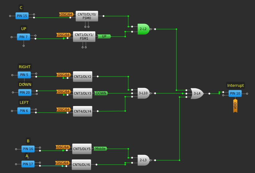
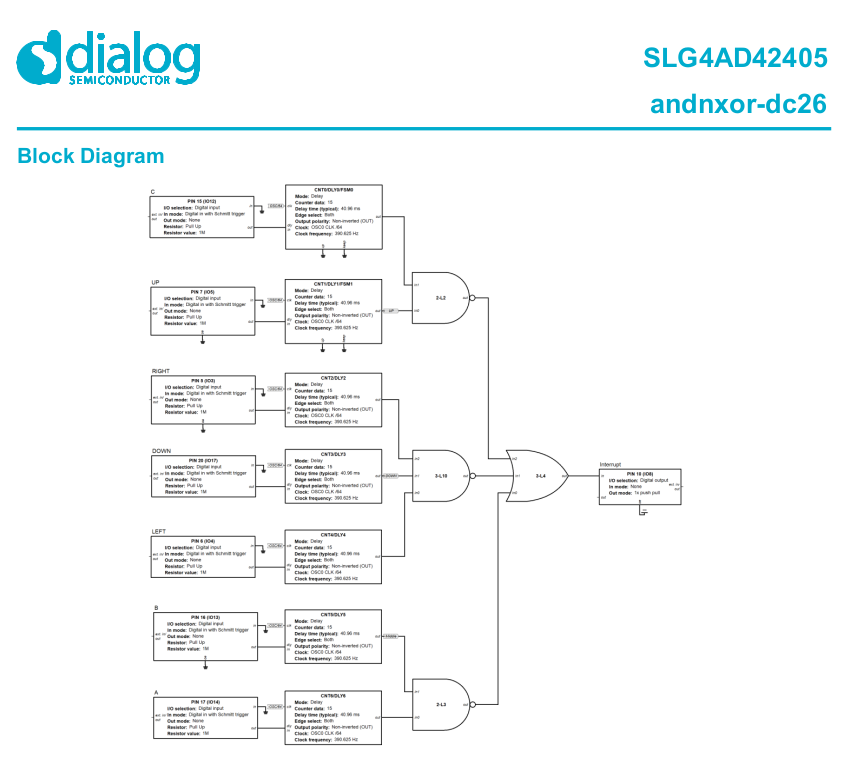
The key is to create a CNT block that is fed by a button. 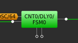
Generating an Interrupt
The next step is to combine the outputs of the debouncers into one pin that goes high when any button is pressed. This is also straightforward.
Using a combination of LUTs I'm able to generate the appropriate high value on Pin 10 when any button is pressed. To get this right it took a lot of trial and error as what I thought was appropriate logic usually ended up backwards from what I was expecting.
But Wait, How Do You Read the Button State?
This is where the magic of the Greenpak comes into play. I2C.
Pins 8 and 9 on my particular Greenpak are hardwired for I2C. By default the Greenpak will listen for address 0x00, which is a poor design choice for shared buses. It can be overridden in the design tool which is exactly what I did as the Greenpak lives on a shared bus on our badge.
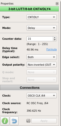
It turns out all the Greenpak is 256 bytes of ROM (writeable once by a dev kit or factory) and 256 bytes of RAM which the ROM is copied into on startup. All LUT states are stored in RAM and addressable over I2C. WOW. You just need to know where to look in the datasheet - it turns out it's more trial and error than I thought.
The CNT blocks from earlier share their output state in a single byte at address 0xF2. Getting the state of each button is a simple bitmask. All the MCU has to do is listen for a rising edge on the interrupt pin then read 0xF2 to check the button states.
Getting our own part number
Something completely unexpected, when Dialog flashed our Greenpaks they also generated a unique part number just for our part then shipped us a datasheet. Pretty cool huh?
 Sadly the part will not be available for ordering. But the generic version, SLG46537V is available and can be flashed using a dev kit. We're not sure how we'll handle the situation where folks want to make their own badge, but open to ideas.
Changing Greenpak Behavior Dynamically
Just as states can be read over I2C, so can configuration be written. In fact, during development we had a minor logic error in the interrupt pin. The interrupt pin was not set to 1x push pull for its output mode and we had already permanently burned the gp5 file to the Greenpak. Womp Womp. 700 times. Double Womp Womp.
The fix was simple. After badge startup, immediately after initializing the Greenpak on I2C (a simple query and ACK to make sure it's there) we write 0x00 to address 0x88 to properly set the configuration of Pin 10. Then everything works from there.
In theory, the entire Greenpak 256 bytes of RAM can be overwritten over I2C. Our original plan was to do just this from the SD card on every start. This created a single point of failure we couldn't accept and instead ended up having the Greenpaks flashed by the factory. In the badge's current boot sequence the SD card isn't guaranteed to be available until very late in the boot. No SD card, no buttons. Alternatively we could embed the 256 bytes of RAM in our firmware and write to the Greenpak early in the boot, which would have worked as well.
We've enjoyed playing with these tiny little devices. Our BOM is slightly reduced as we don't need resistors and capacitors on each button and we got to save some valuable GPIO for other purposes.
Discussions
Become a Hackaday.io Member
Create an account to leave a comment. Already have an account? Log In.