 Fábio Gil
DESCRIPTION
This project is inspired by WRKits (Brazilian Portuguese) and Ben Eater (English) Youtube's channels.
INTRODUCTION
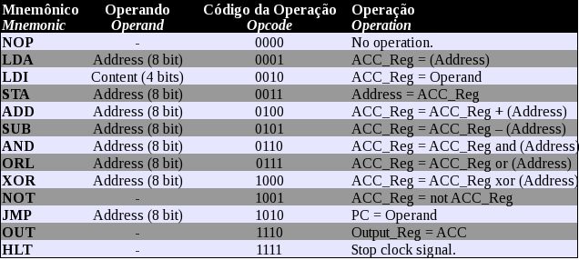
In November/2017, the Engineer Wagner Rambo of WRKits Youtube Channel introduce your project "Build an 8-bit computer" inspired by Ben Eater Youtube Channel when he teach step by step how to build it. All the components is based on TTL, no microcontrollers. In its turn this project is based on SAP (Simple As Possible) Computer of Albert P. Malvino and Jerald A. Brown, both authors of several books about computer architecture.
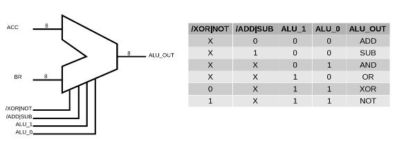
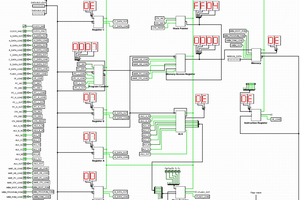
So, I decide build the same computer, following the lessons of Wagner Rambo and Ben Eater, building step by step each modules. I'm an enthusiastic in building electronic device, and for me this project was my one of the biggest challenge. Understanding and building module by module as System Clock, System Reset, Program Counter (PC), Memory Address Register (MAR) and RAM, ALU (Arithmetic and Logic Unit), Accumulator Register (ACC), B Register, Instruction Register, Output Register and Decimal-Display and Instruction Decoder. This is a very basic computer, that make us understand how the microprocessor work. You can see all modules face to face, observing all of ones working together. It's fantastic for me!
So my challenge was launched. All modules of the 8-bit computer were built in order to gain greater knowledge about microprocessors and digital electronic.
And best of all is being able to share all this with you.
LAST UPDATES
- RAM 256 bytes
- Decoder up to 32 instructions
- Microcode updated
- New status register (ZF, CF)
- Conditional jmp implemented
- New instructions: JZ, JNZ, JC, JNC (for conditional jump) and CPA, CPI (for comparison instructions)
NEXT STEPS
No more updates but a new version is planned.
DETAILS
Schematic Diagrams (Current Version Updated):
https://github.com/fgillinux/8bit_computer
Schematic Diagrams (1st Version):
https://github.com/wagner-rambo/arquivos/blob/master/8-bit_computer_18_WR_files.rar
Please, see Project Log bellow.
I'll be back with more videos coming soon. Follow me, take you like (if you really liked) and see you next time!
Thank you!
 Ruud van Falier
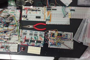
 Andre Baptista
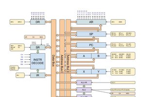
 2-Zons
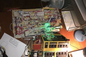
 ammarbhayat28