 zakqwy
I build weird PCBs. Most include copper- and mask-layer graphics, and they often feature complex routed outlines beyond the normal 'this-needs-to-fit-in-an-enclosure'. My tools of choice are Inkscape and KiCad, following a clunky but effective workflow:
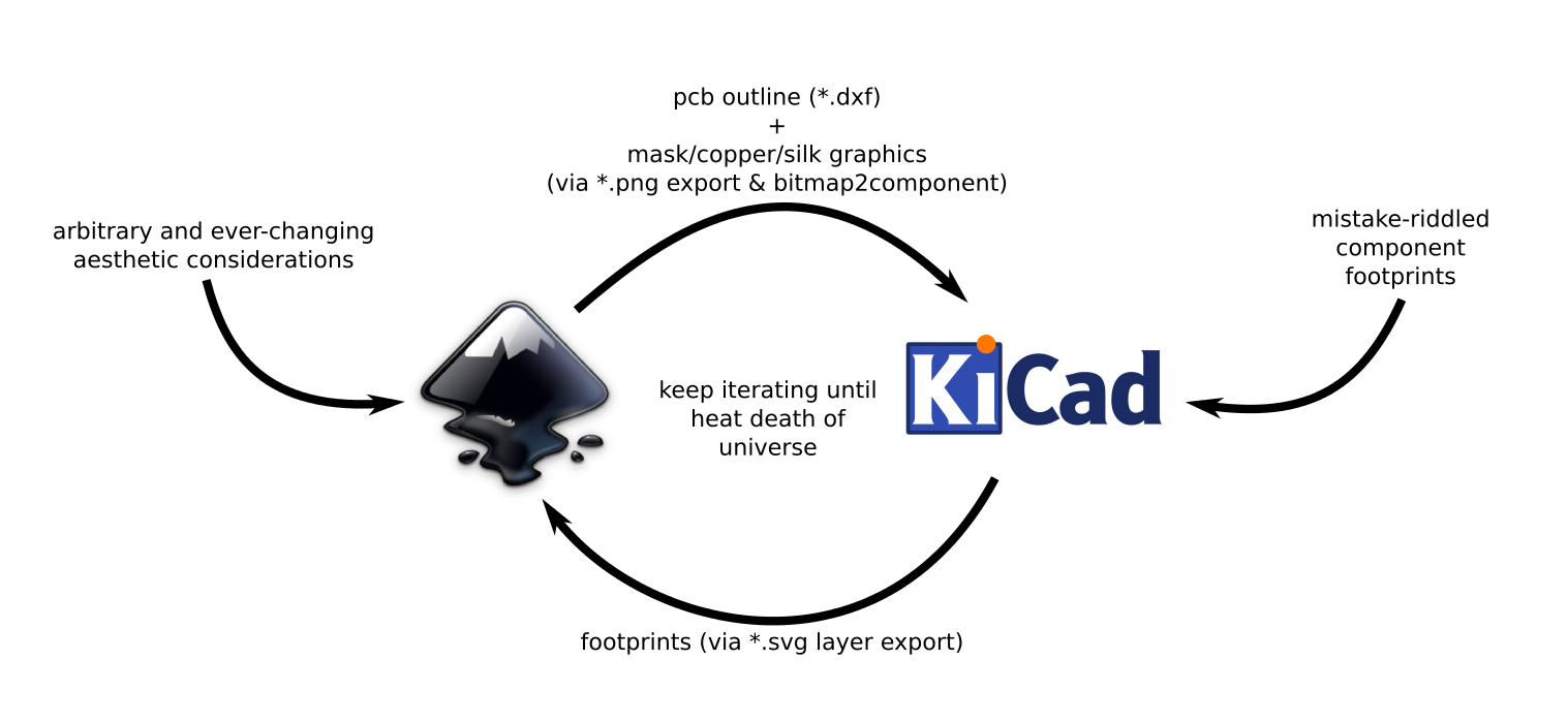
I usually lead with KiCad: throw together a preliminary schematic, make footprints as needed, pull them into Pcbnew, right-click-global-spread-and-place, and export the grid of components into Inkscape. Starting this way ensures the graphical work gets done at scale; most graphics and board outline decisions are bounded by component sizes so it's nice to have this in place up front. Then I put together a first pass at graphics and board outline, export to KiCad, and start high-level routing. Inevitably this results in numerous minor changes that drive the iterative loop until I get sick of the process and send the board out for fabrication. It's no PCBmodE, but I don't think I could live without real-time DRC and push-and-shove routing.
Fundamentally, this process doesn't change with SMT cordwood construction beyond a few extra considerations.
First, cordwood design is confusing. You are designing a circuit in which every component is split in half on the schematic, so it's a lot to keep track of. Between this project and #Splinter, I have found that (a) drawing the schematic (and potentially testing the circuit) in a conventional manner is helpful; and (b) keeping components precisely laid out across from their counterparts is a necessity:
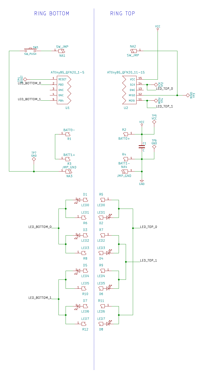
As you can see, I've made a few schematic symbols that are specifically designed to minimize confusion; they even look like they're supposed to interlock across the gap. Remember, KiCad knows how to handle routing on a single PCB, but you have to keep track of routing between the two boards. Note that this means you can't just drop GND and VCC labels everywhere -- keep them on one side if you use them at all!
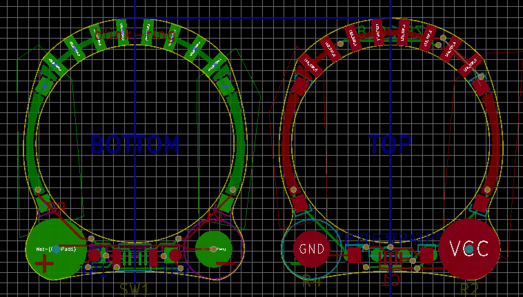
This layout strategy extends to the part placement process, since opposing boards must be inverted and perfectly aligned. The strategy here is to sort parts into two piles, flip half to the back side, align the two PCB outlines to the same grid, and use comment-layer lines and visual cues to ensure component alignment:
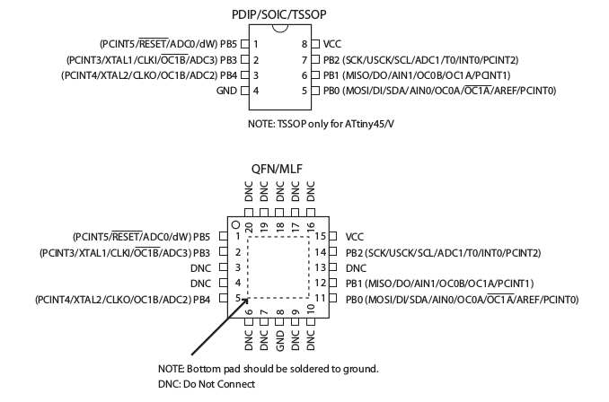
Second, component selection is driven by component length in addition to the usual myriad of other characteristics that one finds via parametric search. SMT cordwood doesn't have the luxury of component leads to absorb small differences between components; everything has to be pretty much spot-on. In the case of this project (and #Splinter for that matter), the key gap of 4mm is based on the dimension of the QFN version of the ATtiny85. Why this part?
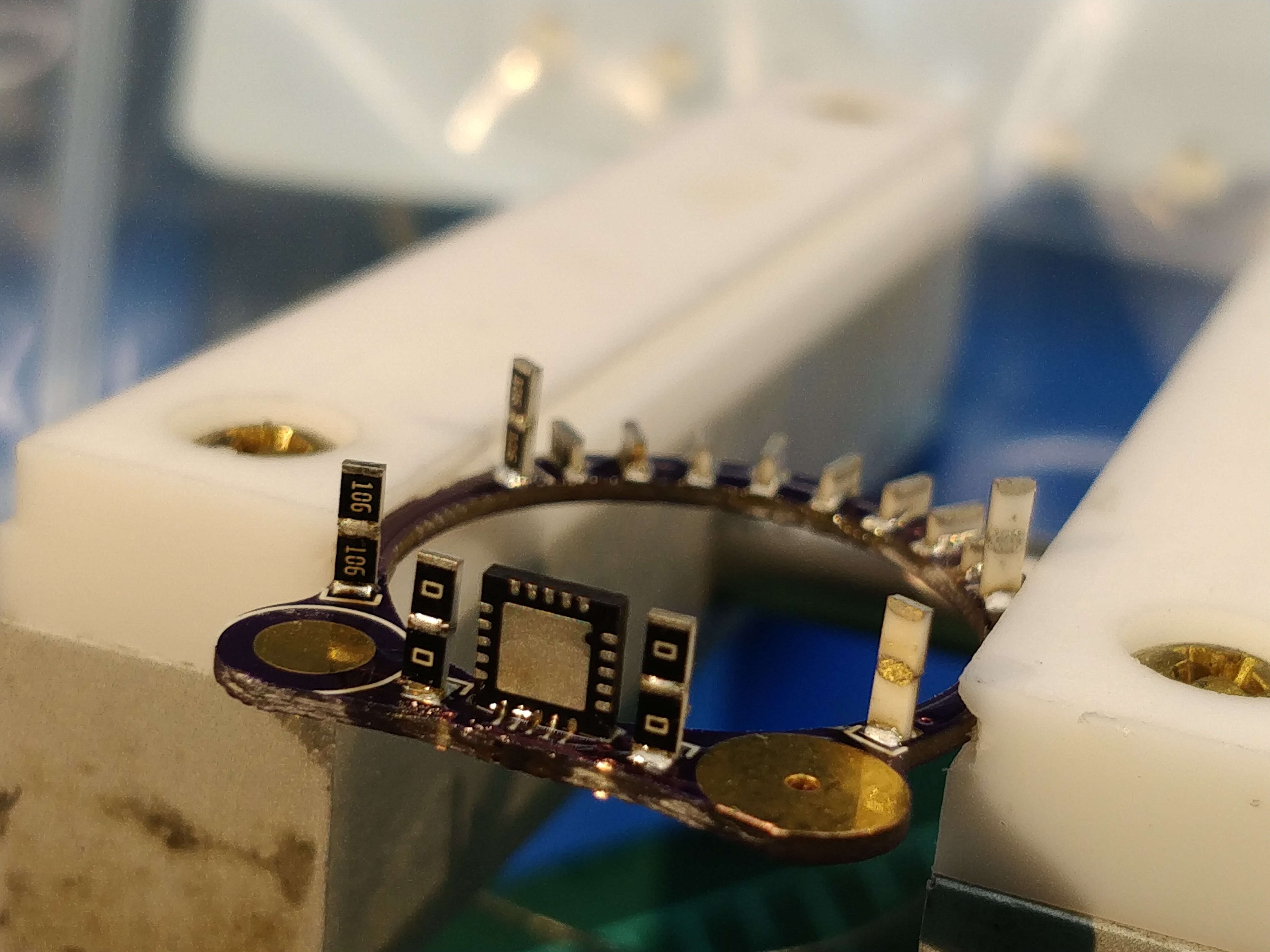 [above, the resistors marked '106' are 10M each -- effectively insulators for the part of the circuit they short out. They are purely structural elements. The resistors marked '0', on the other hand, are jumpers and quite important for circuit operation!]
Once this chip was selected, I worked backwards using Digi-Key's parametric search and a good bit of datasheet examination. I'll put up a Page later on with an updated list, but for now my 4mm span cordwood compatibility guide looks something like this:
- 4mm QFN (i.e. ATtiny85)
- two 0805s, end-to-end (resistors, capacitors, or LEDs)
- one 0508, one 0603, and another 0508, all end-to-end
- a size 10 zinc-air hearing aide battery plus a tiny spring clip
That's all I've used so far, but I'm sure there are other possibilities. One challenge is that there are very few 16xx components (i.e. 4mm width) other than a few oddball inductors, so a bit of math is required when specific component values are required. In the case of this circuit, the switch and the bypass cap were both mounted conventionally.
Saved by the stubby 0508 resistors! Thanks, Rohm!
Third, design-for-manufacture is important, even though these circuits have to be hand-assembled. My strategy thus far has been to build the majority of a given circuit on one side, and then carefully align and tack the boards together before soldering them completely. In the case of this project, the LEDs were added after the two halves were joined -- probably the hardest part of the soldering process. Regardless, it is critical to think about how one will get the soldering iron in to access the component pads during the final assembly process. For a 4mm gap, I try to keep everything within a few millimeters of an accessible PCB edge, and avoid putting components in front of each other entirely.
I'll cover this consideration more as I talk about this project's design in future log updates. I also hope to post a few assembly videos, so stay tuned.
Discussions
Become a Hackaday.io Member
Create an account to leave a comment. Already have an account? Log In.