 Bud Bennett
Feature Set Additions:
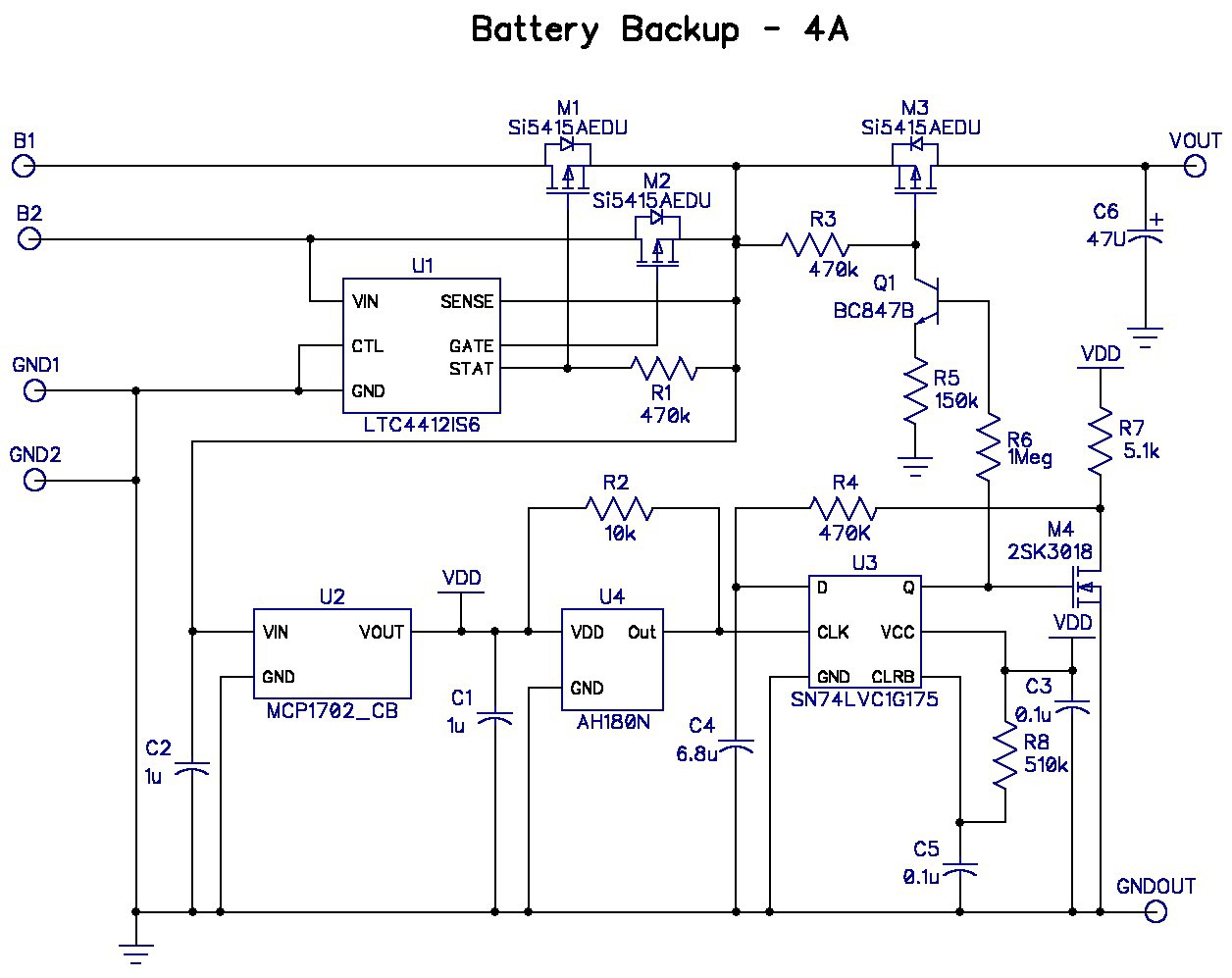
I contacted a engineer friend who is also a RC enthusiast (he designed the LTC4412). He gave me a long list of additional features and helped to settle out the design requirements. I tossed out a lot of his feature set as being too ambitious (like WiFi connectivity), but two of his suggestions merit some consideration here. He was adamant that the circuit not connect the load when a battery is first inserted. This makes sense since it is not expected operation and it could cause damage or injury. His second reasonable requirement was that there be some way of forcing the circuit to connect each battery to the load to test that the system was working correctly. Unfortunately, the LTC4412 could not be made to operate this way and that feature was dropped from consideration.
The Second Pass Circuit:
Sizing the FETs:
It's tempting to just get a big ass FET and be done with it. But there is only so much room on the board and cost is also a constraint. I think it mostly comes down to power dissipation. The PCB is expected to be pretty small (12mm x 25mm or 300 square mm). Using 2 oz. copper will help some, but I expect that the temperature rise with power dissipation will be in the neighborhood of 75-85 °C/W.
The components aren't rated above 85°C, so a 60°C temp rise is all it can tolerate. So maximum power dissipation is 60/85 = 0.7W = Iload^2 2RDSon. Therefore RDSon must be less than 22mΩ (@85°C) for a 4A load. The other FET parameters are VDS ≥ 13V and VGS ≥ 12V (if possible).
After rooting around in the Digikey website I selected the Si5415, which has the following parameters: RDSon < 10mΩ @ VGS = 4.5V, ID < 25A, VDS ≥ 20V, VGS ≥ 8V, $0.63/piece for QTY=10. The downside of this part is the funky PowerPak package, which is a variant of a 2mm x 3mm DFN with an exposed pad. All of the pads are underneath the part. Also, the max VGS is only 8V. I was hoping to get more than 12V, so the VGS will have to be clamped or controlled.
With a RDSon = 12mΩ @ 85°C, the circuit should be able to handle a maximum load current of around 5.5A. The resulting voltage drop across the switches will be 132mV, and less than 100mV with a 4A load. Good enough.
Controlling VGS:
The gate voltage of the FETs must be limited to 8V. The LTC4412 clamps the GATE pin to 7V. The STAT pin is current limited to 10uA (16µA max), which should keep the VGS of M1 below 7.5V, 4.7V typical.
The gate of M3 requires a special level shifter circuit: R3/Q1/R5/R6. The base of Q1 is driven to VDD (3.3V) via R6. If the output voltage is above 10V then Q1 is not saturated and the voltage across R3 is about 3x the voltage across R5 -- about 7.5V. If the output voltage is less than 10V then Q1 saturates and the voltage across R3 is equal to 0.75 VOUT. This gets a bit problematic when VOUT = 3V because the VGS of M3 will drop to 2.25V and RDSon rises to about 15mΩ. But it is doubtful that the servos are going to draw full load at that voltage -- good enough. You could add a zener diode across R3 if 3V operation is a real issue, but it would require higher currents to operate as a predictable clamp.
Power-On-Reset:
Adding the POR was more problematic than anticipated. I really liked the simple D-type flop that I found for the concept schematic, but it did not have a CLR input and so its power up state was unknown. I could not find a D-flop with an inverted output, in a SOT package, that also had a CLR input. I was able to find a D-flop with a CLR, but it has a non-inverted output.
So in typical analog designer fashion I cobbled up a simple inverter -- M4 and R7. And added the POR circuit -- R8 and C5. The CLRB pin will now be held low for about 50ms after power is applied to the inputs, forcing the Q pin of U3 low, which keeps the load switched off.
The other bad thing about using this D-flop is that the quiescent supply current is specified as 10µA. It is only specified as a maximum value over the entire temperature range. I'm hoping that the Iq is much lower at room temperatures, but another 10µA will not break the budget. A 500 mAh battery requires 1.4 years to discharge from a 40µA current. But I'm still hoping to meet the 30µA requirement.
Miscellaneous Additions:
I added a 47µF/16V tantalum at the output. Since it is mounted on the bottom of the board it doesn't really take up any space. The capacitor might keep droop to a minimum when the current draw is light, but at 4A I expect the output to droop 0.7V to 0.8V if a battery is removed or fails. The droop at high load is determined by the body diode of the input FET, which is rated for 25A continuous. If the batteries are sharing the load then that will be the case to minimize output droop to a few tens of mV.
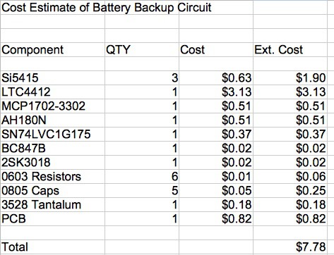
Cost Estimate:
Still under the $10 target:
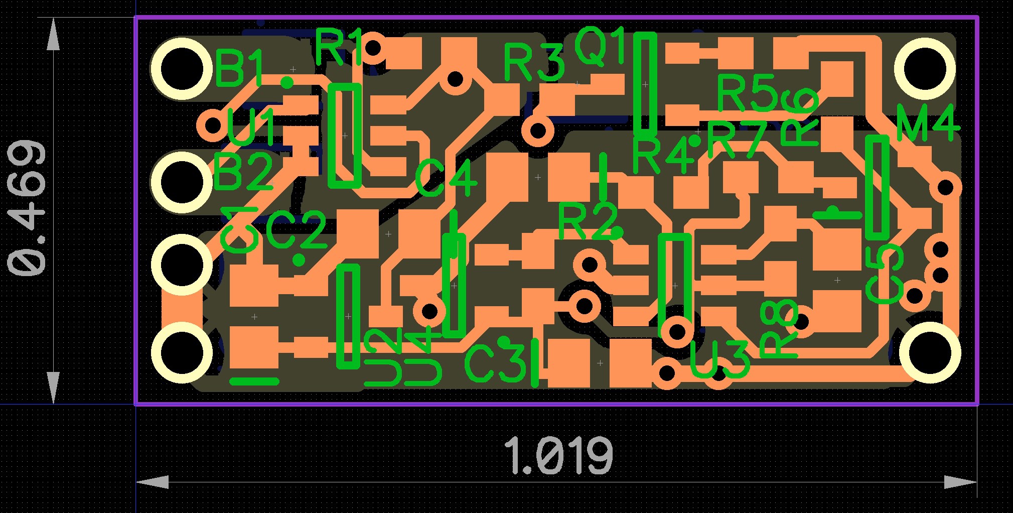
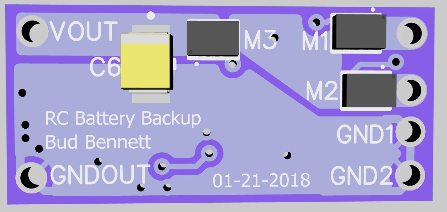
The Layout:
The size of the layout is pretty close to target.
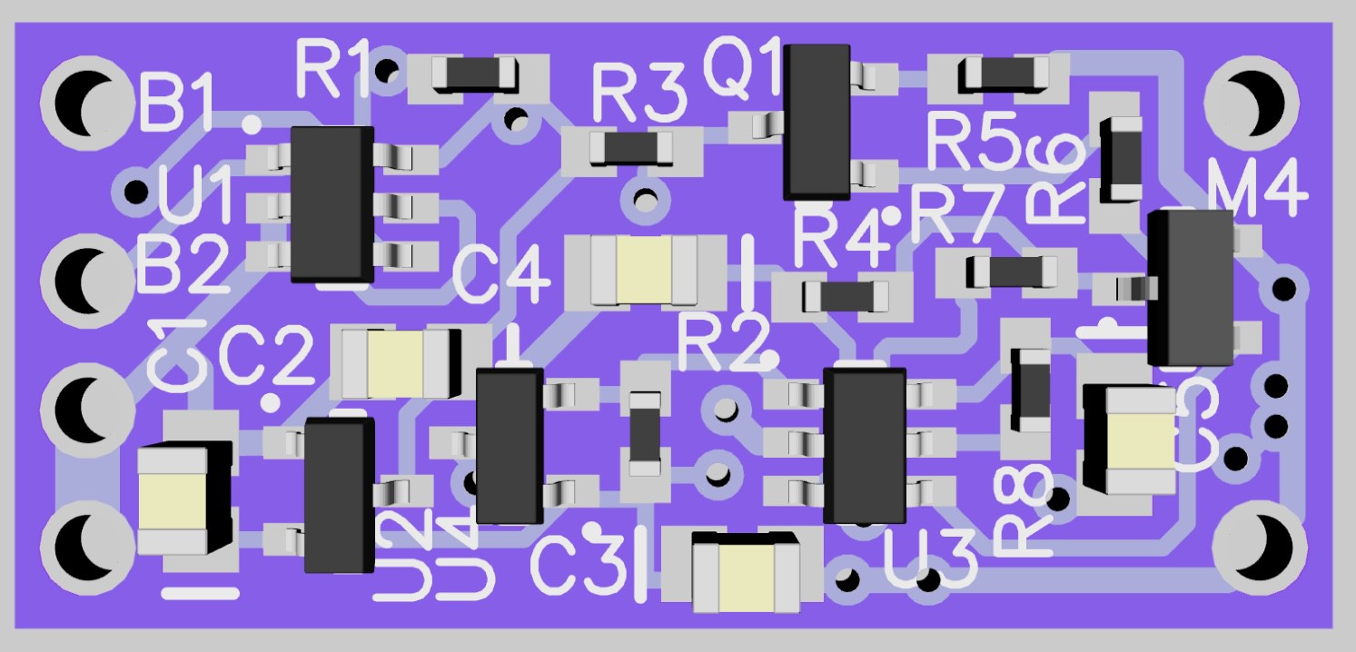
It is easier to get a sense of the populated PCB from the 3D views of top and bottom. The top is pretty well packed. The power FETs were moved to the bottom side to have room for the wide traces.
I'm going to let it age for a few days before pulling the trigger on OSH Park. I don't really expect it to work the first time since simulation was not an option. Something may come up in the interim that wasn't considered properly and prevent wasted time and money.
If you see any glaring error give a shout.
Discussions
Become a Hackaday.io Member
Create an account to leave a comment. Already have an account? Log In.