 Hacker404
I decided that at some stage I need to get some code into this project. I was previously thinking of using an atmega to load boot code to the CPU and then have the CPU boot to SD card.
I am not so sure about using an atmega as a co-processor now that I have decide to use a larger Altera EPM570 CPLD (about 440 macro's).
In any case I need something to get started without going to all the trouble of writing boot loaders.
I decide to hunt around the house for some FLASH as I haven't purchased any.
I found 3 x 32 pin PLCC FLASH chips. 2 were in old mother boards and one was in a CD ROM.
The main board ones were 3.3 Volt only so they were no good to work with a 5 Volt CPU.
The CD ROM one was 5 Volt but it was soldered in -
So I put it (upside down) in an oven tray and heated it until it dropped off the circuit board.
Then when I looked up the specs I found it has the worst of both worlds lol. It has write protection so you can't flash it like you would with older PROMS (just as if they were slow RAM) and also it has *no* Low Pin Count (LPC) interface so I have to use a full blow parallel interface to program it.
I don't have a programmer so I started hunting around to something to expand pin count (like serial in parallel out shift registers) but no good. Then I though ... what about the old Xilinx XC9572XL development board. I could connect that to something ending in 'duino.
As it turned out the the stupid adaptor (dam I hate strip board) that I made was perfect. When I made it, I added extra rows of connectors for different sized breakouts / adaptors. A ZIF socket fitted right in and I had a PLCC32 to DIP adaptor.
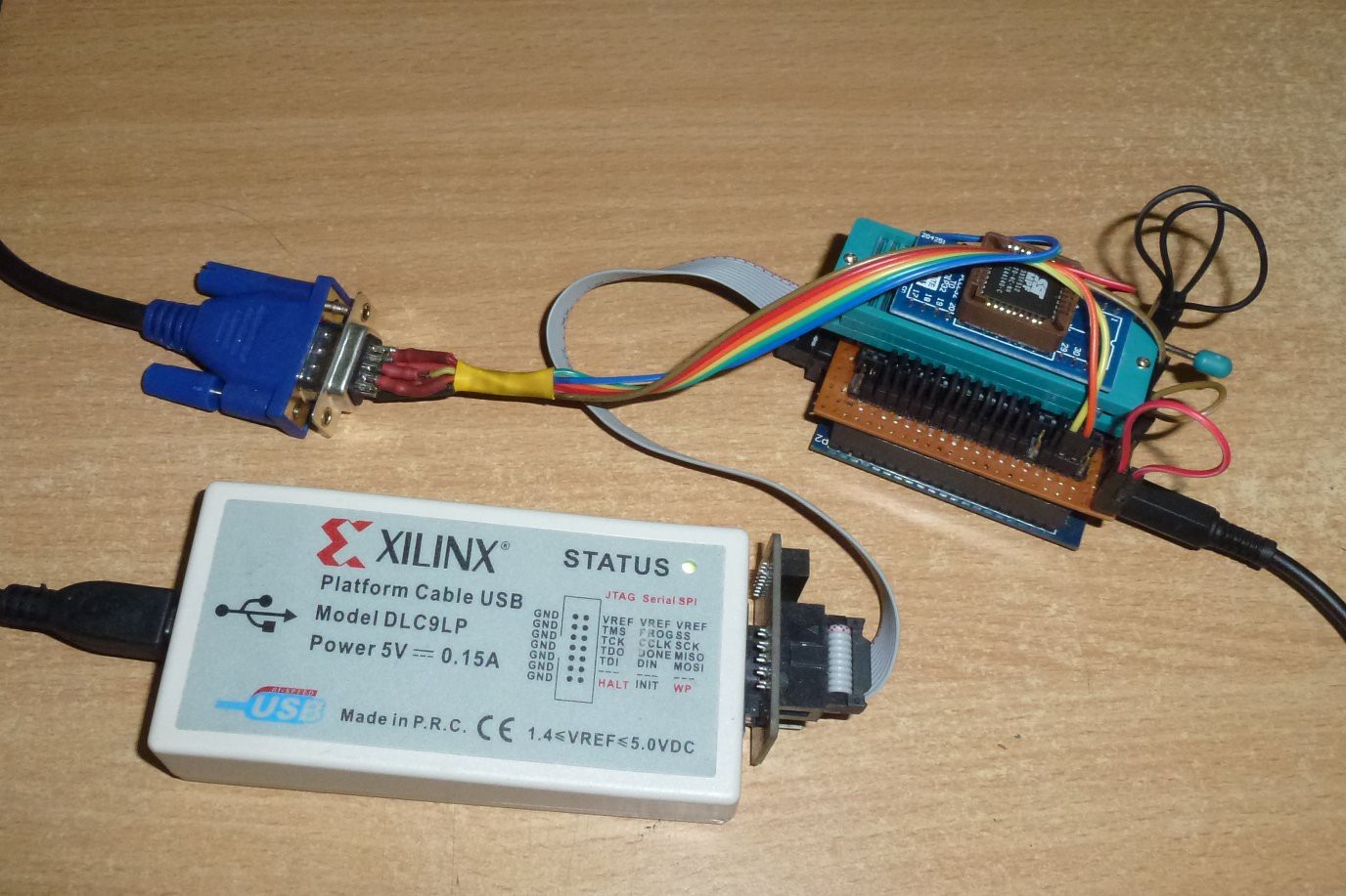
The stack -
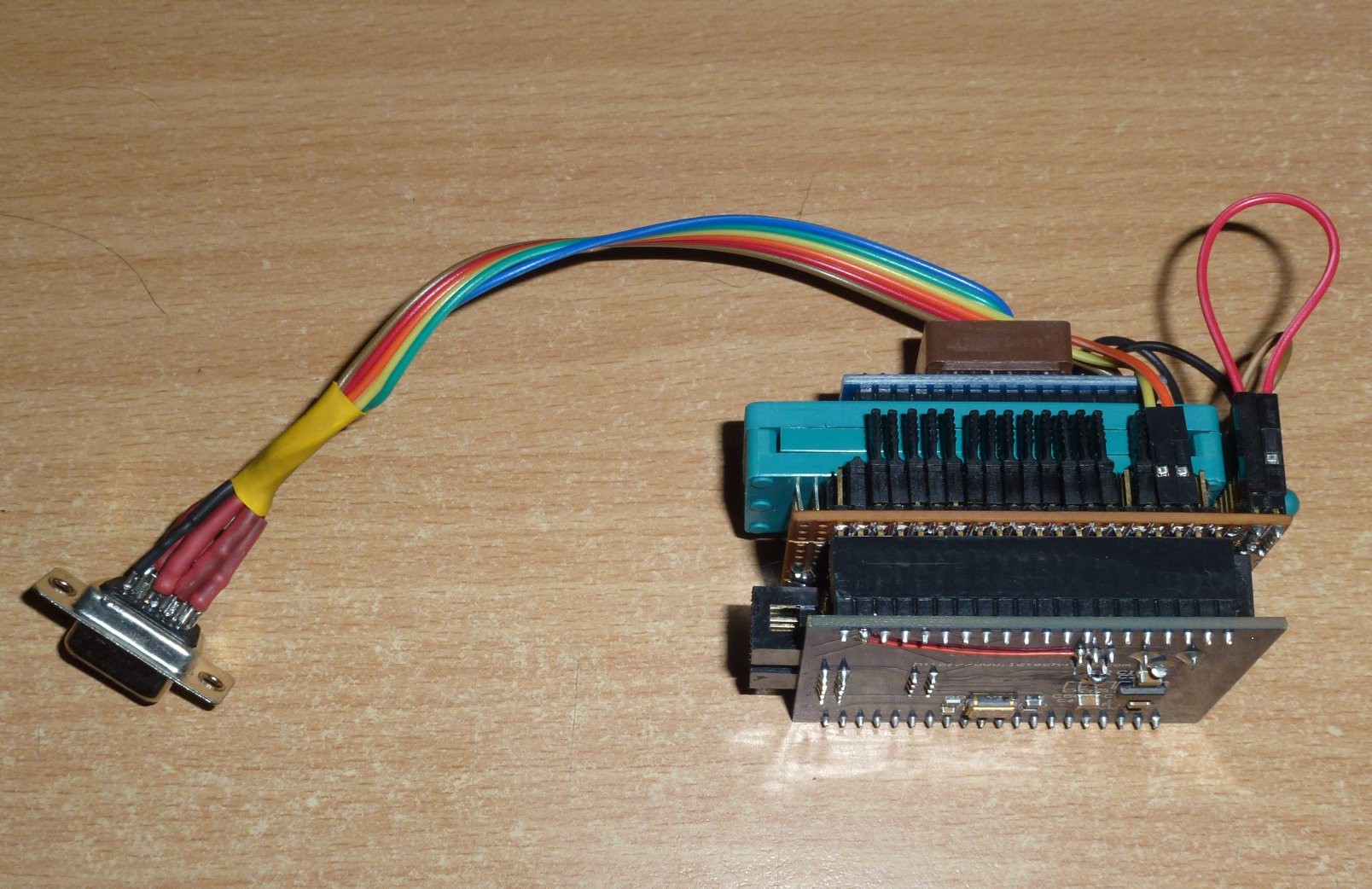
The stack from bottom to top -
- Xilinx XC9574XL development board (5 Volt tolerant 72 Macro's)
- The stupid adaptor that I made to allow connecting CPLD to chips etc with jumper lnks.
- ZIF Socket
- PLCC32 to DIP adaptor
- The target FLASH chip
I though of perhaps making another adaptor to plug this whole contraption into an Arduino UNO but on second thoughts that could cause problems (Stack Overflow??).
Just to see if I got all the connections right and the constraints file right I just quickly changed the old video-out VHDL to work with the FLASH.
Here's what I got -
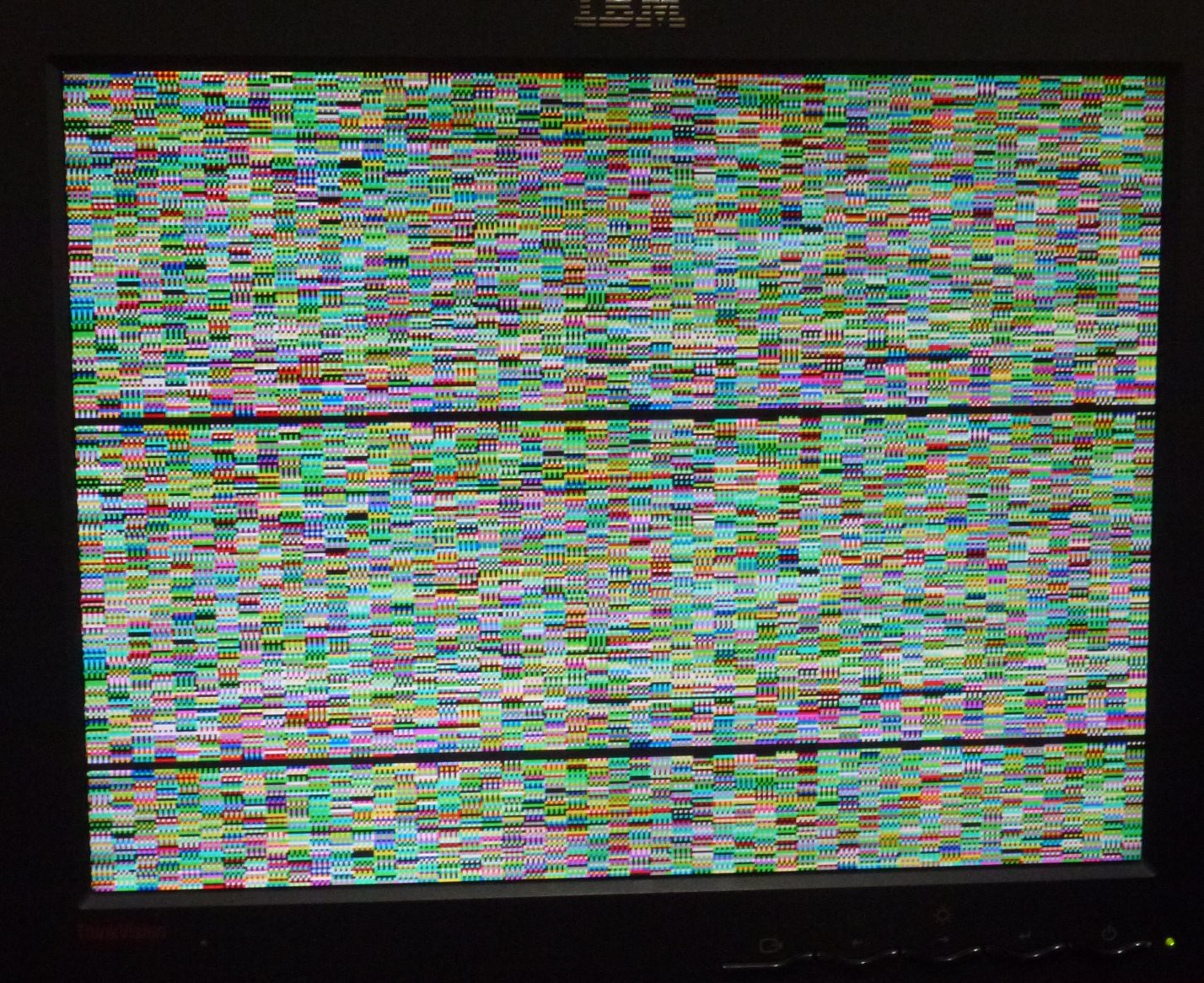
The lines in the picture are because the FLASH chip is much smaller than the SRAM and doesn't have enough room for a full screen.
Then I wrote some VHDL to use the CPLD board as a big shift register. The code is at the end of the log.
It's actualy two shift registers. One is A0-A16 (128KB) + CE + OE + WE + Data out D0-D7.
The second shift register is to read back data from D0-D7.
It has 4 signals to go to the 'duino. Clock, Load, Data Out, Data In.
I am only new to VHDL and I couldn't get LOAD to be asynchronous so it is synchronous to the rising edge of CLOCK. I also had trouble with the tri-state dat bus and I fixed that by using a dedicated 8 bit register.
I am now writing the code for the 'duino to program it and I will update that when it works.
VHDL -
library IEEE;
use IEEE.STD_LOGIC_1164.ALL;

-- I couldn't get a asynchronious load to work so load ended up syncronised to the rising edge of S_CLOCK
-- use process ...

-- note shift register does NOT shift when S_LOAD is high
-- S_CLOCK is rising edge triggered

-- **read flash**
-- serial input WE(1),OE(0),CE(0),-,-,-,A0-15
-- raise S_LOAD, toggle S_CLOCK
-- wait
-- toggle S_CLOCK
-- lower S_LOAD
-- serial read D7 - D0

-- **write flash**
-- serial input WE(0),OE(1),CE(0),-,-,-,A0-15,D0-7
-- raise S_LOAD, toggle S_CLOCK
-- wait
-- perhaps do a readback to confirm

-- **erase flash** as above

entity flash_prog is
    Port (
           -- FLASH pins
           CE      : out    STD_LOGIC; -- Chip Enable   output to FLASH, active low
             OE      : out    STD_LOGIC; -- Output Enable output to FLASH, active low
             WE      : out    STD_LOGIC; -- Write Enable  output to FLASH, active low
             A       : out    STD_LOGIC_VECTOR (15 downto 0); -- Address bus output to FLASH
             D       : inout  STD_LOGIC_VECTOR (7 downto 0); -- bi-directional Data bus to FLASH, controlled by OE
             -- Serial pins
             S_LOAD  : in     STD_LOGIC; -- Serial Latch Enable 0 = shift, 1 = load (synchronious to S_CLK)
          S_CLOCK : in     STD_LOGIC; -- Serial Clock, rising edge triggered
             S_DIN   : in     STD_LOGIC; -- Serial Data Input for outputs to FLASH
          S_DOUT  : out    STD_LOGIC -- Serial Data Output to read back data bus
             );
end flash_prog;

architecture Behavioral of flash_prog is

-- signals
          signal serial_reg : STD_LOGIC_VECTOR (29 downto 0); -- serial register that is copied to latch reg
             signal latch_reg  : STD_LOGIC_VECTOR (29 downto 0); -- all outputs to FLASH
             signal data_reg   : STD_LOGIC_VECTOR (7 downto 0); -- reads back from data bus
      -- serial_reg and latch_reg
      -- (0 to 15)  - A(0 to 15)
      -- (16)       - A(16) not implemented
      -- (17)       - A(17) not implemented
      -- (18)       - A(18) not implemented
      -- (19)       - CE active low
      -- (20)       - OE active low
      -- (21)       - WE active low
      -- (22 to 29) - D(0 to 7) for output only
      -- S_DI => A0 - A15, -, -, -, CE, OE, WE, D0 - D7
      -- '0' => D0 - D7 => S_DO

begin

process (S_CLOCK, S_LOAD)
  begin
  if (S_CLOCK'EVENT AND S_CLOCK = '1') then -- rising edge
    if (S_LOAD = '0') then -- shift
       serial_reg(29 downto 1) <= serial_reg(28 downto 0);
        serial_reg(0) <= S_DIN;
        data_reg(7 downto 1) <= data_reg(6 downto 0);
        data_reg(0) <= '0';
     else -- latch
       latch_reg(29 downto 0) <= serial_reg(29 downto 0);
        data_reg(7 downto 0) <= D(7 downto 0);
     end if;
  end if;
end process;


-- serial interface
  S_DOUT <= data_reg(7);

-- FLASH interface
  CE <= latch_reg(19);
  OE <= latch_reg(20);
  WE <= latch_reg(21);
  A(15 downto 0) <= latch_reg(15 downto 0);

-- tristate data bus
  D(7 downto 0) <= latch_reg(29 downto 22)
  when (latch_reg(20) = '1')
  else "ZZZZZZZZ";


end Behavioral;
Constraints (Xilinx Format) -
# Constraints for SST 39SF512 FLASH EEPROM (64K x 8, 5V, 70ns)


# 3.3 Volts
#   5 Volts
#NET "CLK"        LOC = "p1";
#NET ""        LOC = "p2";
NET "A(15)"        LOC = "p3";
NET "A(12)"        LOC = "p5";
NET "A(7)"        LOC = "p6";
NET "A(6)"        LOC = "p7";
NET "A(5)"        LOC = "p8";
NET "A(4)"        LOC = "p12";
NET "A(3)"        LOC = "p13";
NET "A(2)"        LOC = "p14";
NET "A(1)"        LOC = "p16";
NET "A(0)"        LOC = "p18";
NET "D(0)"        LOC = "p19";
NET "D(1)"        LOC = "p20";
NET "D(2)"        LOC = "p21";
NET "S_CLOCK"    LOC = "p22";
NET "S_LOAD"    LOC = "p23";
# GND

# GND
NET "S_DIN"        LOC = "p44";
NET "S_DOUT"    LOC = "p43";
NET "WE"            LOC = "p42";
#NET ""            LOC = "p41";
NET "A(14)"        LOC = "p40";
NET "A(13)"        LOC = "p39";
NET "A(8)"        LOC = "p38";
NET "A(9)"        LOC = "p37";
NET "A(11)"        LOC = "p36";
NET "OE"        LOC = "p34";
NET "A(10)"        LOC = "p33";
NET "CE"        LOC = "p32";
NET "D(7)"        LOC = "p31";
NET "D(6)"        LOC = "p30";
NET "D(5)"        LOC = "p29";
NET "D(4)"        LOC = "p28";
NET "D(3)"        LOC = "p27";
#   5 Volts
# 3.3 Volts
Well!, In the constraints file (above) I had A(1) and A(2) repeated. The second A(1), A(2) should have been D(1), D(2). That took a long time to find.
Here's the 'duino code. It's just Proof of Concept but it works. It needs a verify.
#define S_CLOCK 2
#define S_LOAD  3
#define S_DIN   4
#define S_DOUT  5


/*
-- note shift register does NOT shift when S_LOAD is high
-- S_CLOCK is rising edge triggered

-- **read flash**
-- serial input WE(1),OE(0),CE(0),-,-,-,A0-15
-- raise S_LOAD, toggle S_CLOCK
-- wait
-- toggle S_CLOCK
-- lower S_LOAD
-- serial read D7 - D0

-- **write flash**
-- serial input D0-7, WE(0), OE(1), CE(0), -, -, -, A0-15
-- raise S_LOAD, toggle S_CLOCK
-- wait
-- perhaps do a readback to confirm

-- **erase flash** as above
*/

char hx[] = "0123456789ABCDEF";

byte values[256];

void to_hex(long dec, int digits)
  {
  for(int index = 0; index < digits; index++)
    {
    hx[digits - index - 1] = to_hex_digit(dec & 15);
    dec = dec >> 4;
    }
  hx[digits] = 0;
  }


int to_hex_digit(int dec)
  {
  dec = dec & 15;
  dec = dec + 48;
  if(dec > 57)
    {
    dec = dec + 7;
    }
  return dec;
  }


void setup()
  {
  pinMode(S_CLOCK, OUTPUT);
  pinMode(S_LOAD, OUTPUT);
  pinMode(S_DOUT, INPUT);
  pinMode(S_DIN, OUTPUT);
  Serial.begin(115200);
  delay(100);
  }


void loop()
  {
  //blink_A15();
  long mem_start = 0;
  //sector_erase(13);
  chip_erase();
  //write_address(0x13, 0xAB);
  //write_address(mem_start, 0);
  //write_address(mem_start+1, 255);
  //      data, WE, OE, CE, address
  long mem_count = 65536;
  int show_address_counter = 63;
  serial_out(0, 1, 1, 1, 0);
  for(long address = mem_start; address < (mem_start + mem_count); address++)
    {
    show_address_counter++;
    if(show_address_counter == 64)
      {
      show_address_counter = 0;
      to_hex(address, 4);
      Serial.println("");
      Serial.print(hx);
      Serial.print("  ");
      }
    int one_byte = read_address(address);
    values[one_byte] = 1;
    to_hex(one_byte, 2);
    Serial.print(hx);
    Serial.print("");
    //address = address + 15;
    }
  Serial.println("");
  Serial.println("0123456789ABCDEF");
  for(int index1 = 0; index1 < 16; index1++)
    {
    for(int index2 = 0; index2 < 16; index2++)
      {
      int dec = index1 * 16 + index2;
      if(values[dec] != 1)
        {
        Serial.print("X");
        }
      else
        {
        Serial.print(".");
        }
      }
    Serial.println("");
    }
  for(; 1 == 1;){}
  }


void signal_delay()
  {
  //  This may be needed for long wire connections
  //delayMicroseconds(10);
  }


void sector_erase_delay()
  {
  delay(20); // 10mS
  }


void chip_erase_delay()
  {
  delay(40); // 20mS
  }

void write_delay()
  {
  delayMicroseconds(60);
  }


void toggle_S_CLOCK()
  {
  digitalWrite(S_CLOCK, HIGH);
  signal_delay();
  digitalWrite(S_CLOCK, LOW);
  signal_delay();
  }


void toggle_S_LOAD()
  {
  digitalWrite(S_LOAD, HIGH);
  signal_delay();
  toggle_S_CLOCK();
  digitalWrite(S_LOAD, LOW);
  signal_delay();
  }


int serial_in_bit()
  {
  int one_bit;
  if(digitalRead(S_DOUT) == LOW)
    {
    one_bit = 0;
    }
  else
    {
    one_bit = 1;
    }
  toggle_S_CLOCK();
  return one_bit;
  }


int serial_in_byte()
  {
  int one_byte;
  int one_bit;
  for(int index = 7; index >= 0; index--)
    {
    one_bit = serial_in_bit();
    one_byte = (one_byte | (one_bit << index));
    }
  return one_byte;
  }


void serial_out_bit(int one_bit)
  {
  if(one_bit == 0)
    {
    digitalWrite(S_DIN, LOW);
    }
  else
    {
    digitalWrite(S_DIN, HIGH);
    }
  toggle_S_CLOCK();
  }


void serial_out(int data, int we, int oe, int ce, long add)
  {
  for(int index = 7; index >= 0; index--)
    {
    int one_bit = (data & (1 << index));
    serial_out_bit(one_bit);
    }
  serial_out_bit(we);
  serial_out_bit(oe);
  serial_out_bit(ce);
  serial_out_bit(0);
  serial_out_bit(0);
  serial_out_bit(0);
  for(int index = 15; index >= 0; index--)
    {
    int one_bit = (add & (1 << index));
    serial_out_bit(one_bit);
    }
  toggle_S_LOAD();
  }


int read_address(long add)
  {
  int one_byte;
  //      data, WE, OE, CE, address
  //serial_out(0, 1, 1, 1, 0);
  //serial_out(0, 1, 0, 0, add);
  //serial_out(0, 1, 0, 0, add);
  serial_out(0, 1, 0, 0, add);
  toggle_S_LOAD();
  one_byte = serial_in_byte();
  return one_byte;
  }


void write_address(long add, int data)
  {
  //      data, WE, OE, CE, address
  serial_out(0xAA, 1, 1, 0, 0x5555);
  serial_out(0xAA, 0, 1, 0, 0x5555);

  serial_out(0x55, 1, 1, 0, 0x2AAA);
  serial_out(0x55, 0, 1, 0, 0x2AAA);

  serial_out(0xA0, 1, 1, 0, 0x5555);
  serial_out(0xA0, 0, 1, 0, 0x5555);

  serial_out(data, 1, 1, 0, add);
  serial_out(data, 0, 1, 0, add);

  serial_out(data, 1, 1, 0, add);

  write_delay();
  }


void sector_erase(int sector)
  {
  sector = sector & 15;
  sector = (sector << 12);
  //      data, WE, OE, CE, address
  serial_out(0xAA, 1, 1, 0, 0x5555);
  serial_out(0xAA, 0, 1, 0, 0x5555);

  serial_out(0x55, 1, 1, 0, 0x2AAA);
  serial_out(0x55, 0, 1, 0, 0x2AAA);

  serial_out(0x80, 1, 1, 0, 0x5555);
  serial_out(0x80, 0, 1, 0, 0x5555);

  serial_out(0xAA, 1, 1, 0, 0x5555);
  serial_out(0xAA, 0, 1, 0, 0x5555);

  serial_out(0x55, 1, 1, 0, 0x2AAA);
  serial_out(0x55, 0, 1, 0, 0x2AAA);

  serial_out(0x30, 1, 1, 0, sector);
  serial_out(0x30, 0, 1, 0, sector);

  serial_out(0x30, 1, 1, 0, sector);

  sector_erase_delay();
  }


void chip_erase()
  {
  serial_out(0xAA, 1, 1, 0, 0x5555);
  serial_out(0xAA, 0, 1, 0, 0x5555);

  serial_out(0x55, 1, 1, 0, 0x2AAA);
  serial_out(0x55, 0, 1, 0, 0x2AAA);

  serial_out(0x80, 1, 1, 0, 0x5555);
  serial_out(0x80, 0, 1, 0, 0x5555);

  serial_out(0xAA, 1, 1, 0, 0x5555);
  serial_out(0xAA, 0, 1, 0, 0x5555);

  serial_out(0x55, 1, 1, 0, 0x2AAA);
  serial_out(0x55, 0, 1, 0, 0x2AAA);

  serial_out(0x10, 1, 1, 0, 0x5555);
  serial_out(0x10, 0, 1, 0, 0x5555);

  serial_out(0x10, 1, 1, 0, 0x5555);

  chip_erase_delay();
  }


byte data[] = {0x00, 0x00, 0x00} // truncated this line was 16,000 Bytes


/*

// some diagnostic routines


void blink_WE()
  {
  //      data, WE, OE, CE, address
  for(; 1 == 1;)
    {
    serial_out(0, 0, 1, 1, 0);
    delay(200);
    serial_out(0, 1, 1, 1, 0);
    delay(200);
    }
  }


void blink_OE()
  {
  //      data, WE, OE, CE, address
  for(; 1 == 1;)
    {
    serial_out(0, 1, 0, 1, 0);
    delay(200);
    serial_out(0, 1, 1, 1, 0);
    delay(200);
    }
  }


void blink_CE()
  {
  //      data, WE, OE, CE, address
  for(; 1 == 1;)
    {
    serial_out(0, 1, 1, 0, 0);
    delay(200);
    serial_out(0, 1, 1, 1, 0);
    delay(200);
    }
  }


void blink_D0()
  {
  //      data, WE, OE, CE, address
  for(; 1 == 1;)
    {
    serial_out(1, 1, 1, 1, 0);
    delay(200);
    serial_out(0, 1, 1, 1, 0);
    delay(200);
    }
  }


void blink_D7()
  {
  //      data, WE, OE, CE, address
  for(; 1 == 1;)
    {
    serial_out(128, 1, 1, 1, 0);
    delay(200);
    serial_out(0, 1, 1, 1, 0);
    delay(200);
    }
  }


void blink_A0()
  {
  //      data, WE, OE, CE, address
  for(; 1 == 1;)
    {
    serial_out(0, 1, 1, 1, 1);
    delay(200);
    serial_out(0, 1, 1, 1, 0);
    delay(200);
    }
  }


void blink_A15()
  {
  //      data, WE, OE, CE, address
  for(; 1 == 1;)
    {
    serial_out(0, 1, 1, 1, 32768);
    delay(200);
    serial_out(0, 1, 1, 1, 0);
    delay(200);
    }
  }
*/
I will modify the VHDL so that it works with larger FLASH chips. The existing VHDL works for a 64KB (512Kb) chip. I will add 3 addresses so it can do 128KB (1Mb), 256KB (2Mb) and 512KB (4Mb) chips as well. I want to use a 512KB (4Mb) chips but I haven't yet found a 5 Volt version, perhaps they don't exist.
I will also modify the 'duino code for larger chips and fix it up. I want to see if I can simply drop files into the serial monitor and program that way. I can only store 16KB in the 'duino flash so it takes 4 sessions just to program 64KB.
Discussions
Become a Hackaday.io Member
Create an account to leave a comment. Already have an account? Log In.