0%
0%
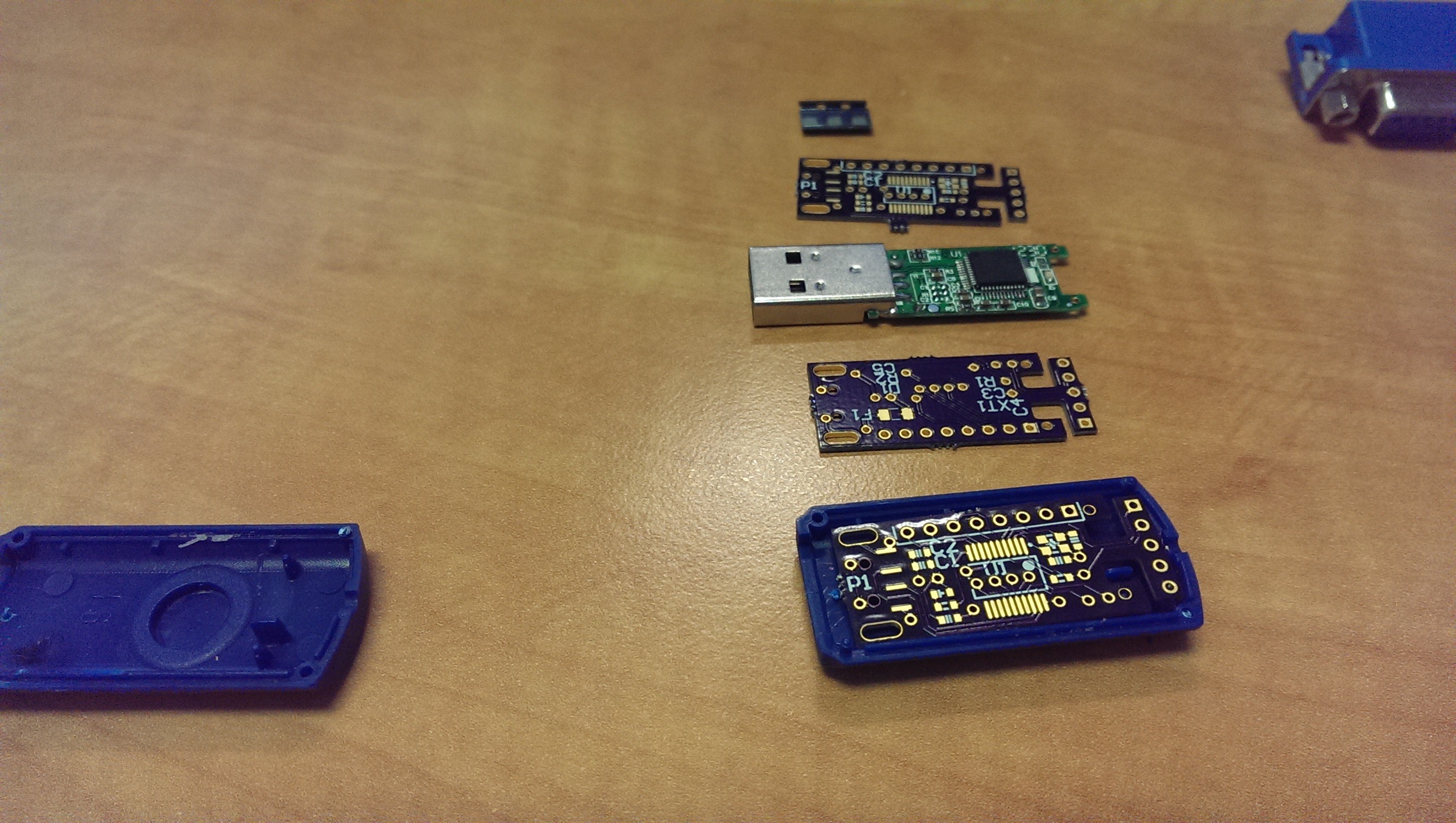
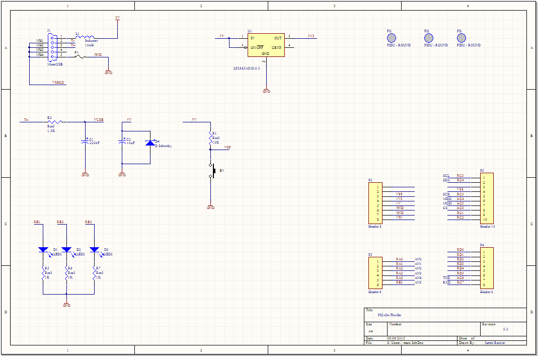
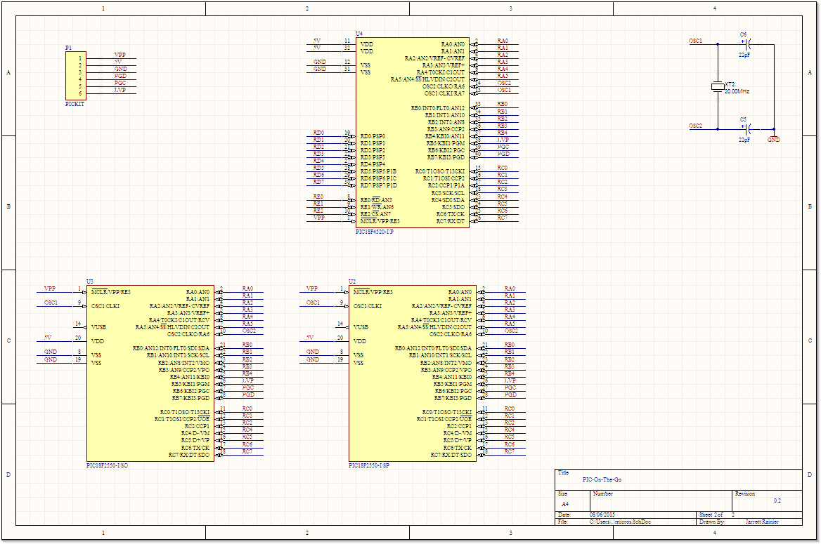
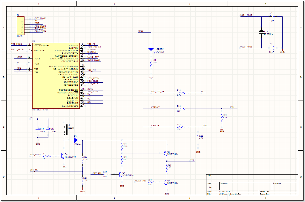
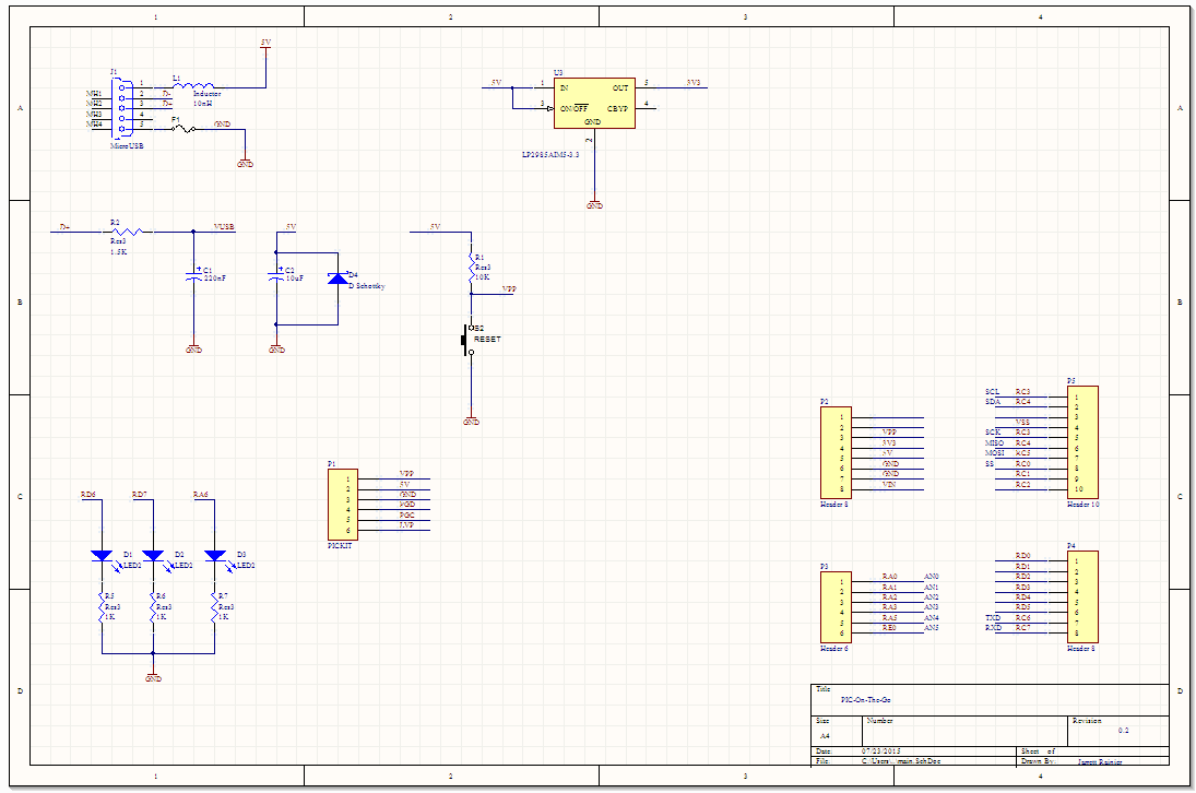
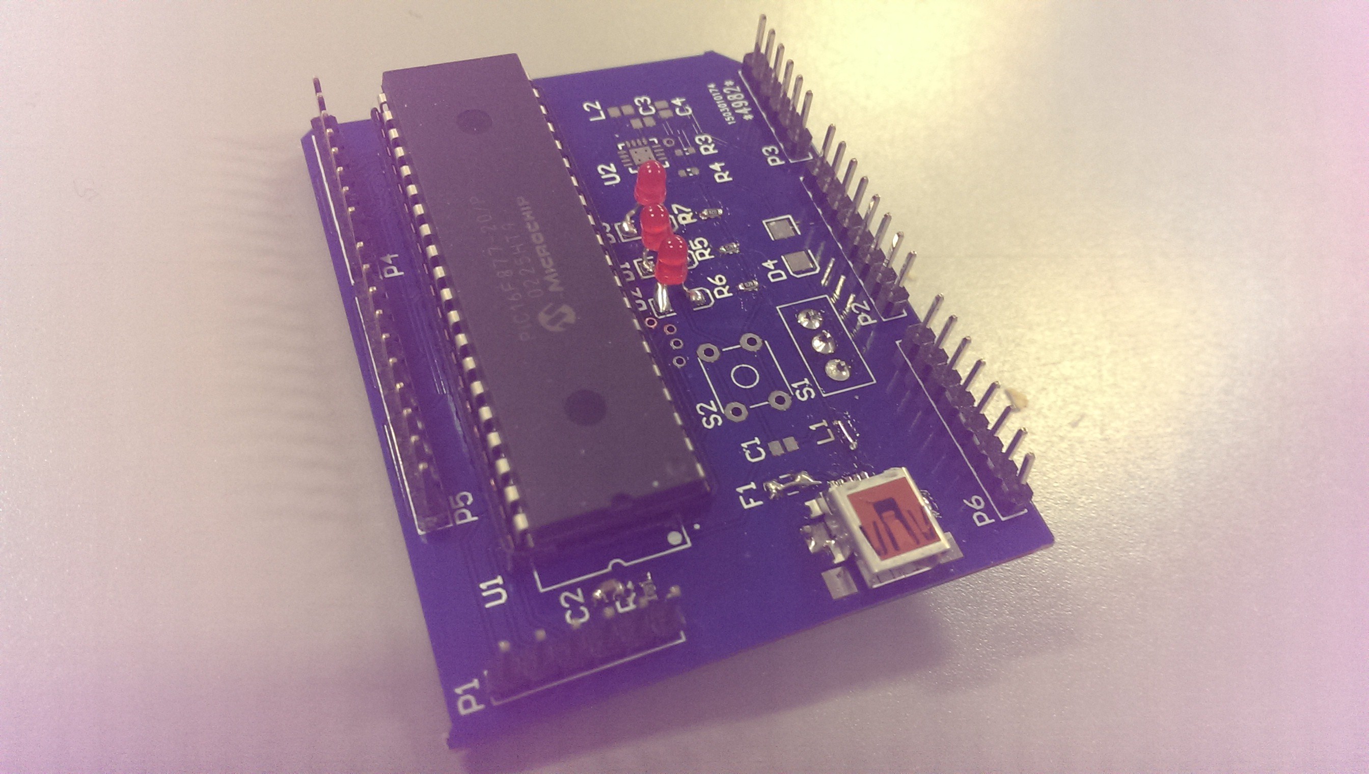
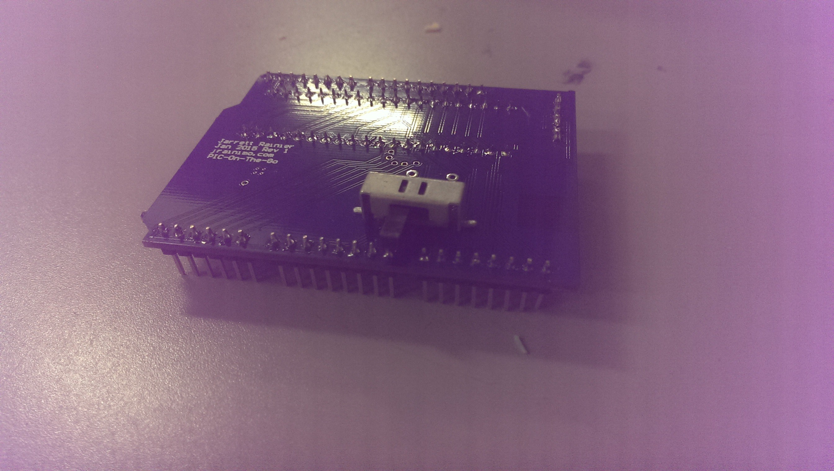
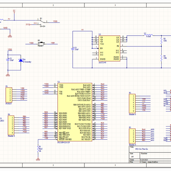
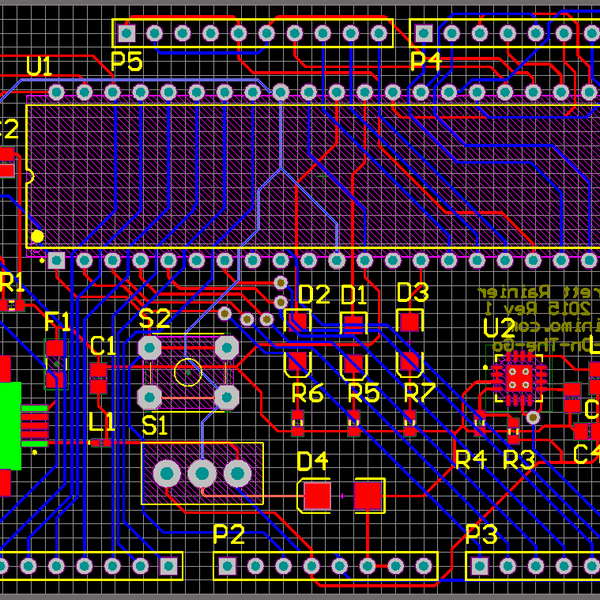
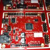
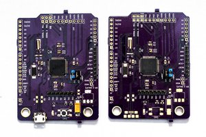
PIC-On-The-Go
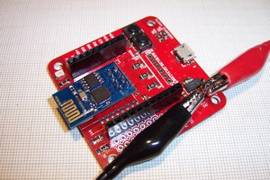
PIC Microcontroller dev boards, in unusual cases
 Jarrett
Become a Hackaday.io member
Already have an account? Log in.
Just one more thing
To make the experience fit your profile, pick a username and tell us what interests you.
Pick an awesome username
hackaday.io/
Your profile's URL: hackaday.io/username. Max 25 alphanumeric characters.
Pick a few interests
Projects that share your interests
People that share your interests


 Stefan Lochbrunner
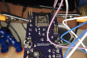
 Casual Cyborg
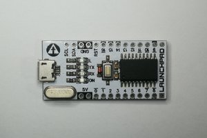
 Clyde D. Corpuz
"I am stubborn as all hell and just want to use my PICs" -- You, I like you.
Check out the Mikroe dev boards. I personally like the Clicker2 boards and the Mikroe Bus add on Click boards (Aka: Shields) are great too... pretty much the same stuff you find on any arduino shield, lots of variaty.
The only draw back ive seen is that the PIC choice for these boards does not have any internal EEPROM... which sucks. other than that.. awesome boards.