Christoph
General thoughts
Commonly used to switch Nixie Tubes is the K155ID1 (74141). Nice: it's also a BCD to decimal converter. Not Nice: You can only get old stock which has been lying around for decades. And since Nixies are getting more popular prices increase. So let's build our own.
Problem are the voltages. Nixie Tubes have an anode voltage of around 100-200V. Tricky question: What's the cathode voltage when switched off? I'm serious, what is the answer? Since there is no physical connection between cathode and anode it's something in between depending on the switching state. If you're not sure expect the worst case, so I wanted a way to safely switch 200-300V even so I assume the real Voltage drop is much lower.
That's why I will use the MPSA 42 NPN High Voltage Transistor which has a maximum Collector-Emitter Voltage of 300V. You might simply connect on transistor to one digital IO of your favorite microcontroller. But that scales badly. One Nixie (Digits 0-9 and Dot): 11 I/Os, two Nixies: 22 I/Os, and so on.
Lets use a shift register. Google for TPIC6B595 if you want to check out the datasheet. Any other shift register will be fine too, I used what I had available. Let's recall how a shift register works.
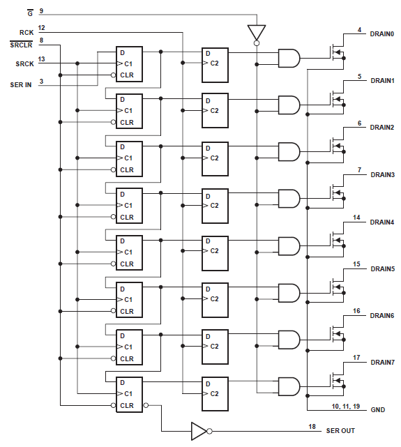
Note that tis very special one has FETs at it's output to driver higher loads. You have a single one-bit serial data input (SERI IN) feeding the first One-Bit-Storage (D-FlipFlop). The Output of the FlipFlop feeds the next input and so on. Typically you have a set of eight Bit-Storages since we live in a binary world. The last Bit-Storage outputs it's value as "SER OUT" for cascading multiple shift-registers (or other uses). Applying a clock (SRCK) makes every bit-storage "save" the current input state (high/low) and deliver it to the output. By cascading the Bit storages in a serial way we created a shift register. Since the output word (8 bit) of the serial cascaded array (may) change/s at every clock you want to have control about when to deliver the output to the driving side (right hand FETs). That's why there are an additional 8 D-FlipFlops which you clock (RCK) after your serial data is completely clocked into the input side. Everything else is just convenience. SRCLR\ lets you asynchronously (timing unrelated to SRCK) clear the input stage (set all to 0 or low). You can also clock in 8 zeros. G\ disables the output stage of driving the FETs. For basic applications you need SER IN, SRCK, RCK. Apply a constant 0 (ground) to G\ and SRCLR\ when not in use.
That's a maximum of 5 IO/s vs. 11 per Tube. Half way there!
Looking at Datasheet
Datasheets are not always easy to read, especially when you're not too familiar with the technical background. Check the maximum ratings. Supply voltage (max. 7V) and logic input voltage (-0.3 to 7V). What controller are you using? What's the IO output and supply voltage? Crosscheck the recommended values. Supply voltage Vcc: 4.5-5.5V. When using a more modern controller running with 3.3V is there 5V available at all? Check the Voltage levels for High level input 0.85*Vcc (4.25V@5V) and low level input 0.15*Vcc (0.75V@5V). Check timings. Setup time, Hold time, Pulse duration (20,20,40ns).
Do you meet all criteria? I am using an ARM Cortex Board running on 3,3V. 5V is available from USB port. The 3.3V IO output voltage is below the recommended 4.25V. Truth is, it works with 3.3V as well but that's out of specs. So don't do for device that you depend on. In that case use a level shifter. What about the timings? How long does it take to switch an IO? How do you check that? Think of your clock frequency of your microcontroller. In my case (Stellaris Launchpad) it is 80MHz the fastest possible switching time would be a single instruction (1/80MHz = 12.5ns). Well that is a close one on this uC. Since I am using some libraries to set the IOs there's additional timing overhead coming from calling and returning functions etc. If the code is extremely optimized you may run into problems and if you're running much faster controllers (like the STM32F4Discovery running on 168MHz) you need to ensure the timing by artificially delays. Coming from an Arduino world check out delayMicroseconds().
Wiring
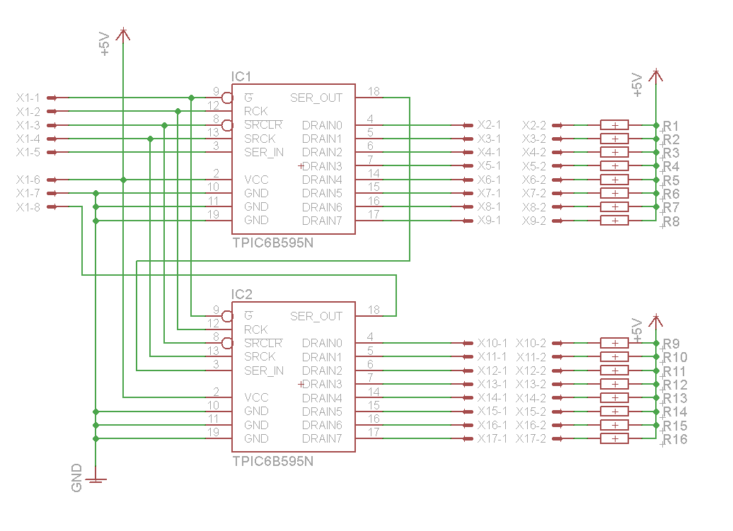
X1 goes to your controller connecting G\, RCK, SRCK\, SER IN, SER OUT and Supply. X2-X17 are output pins to switch the Nixie cathodes. I use octocouplers as described here to swich the cathodes: I use octocouplers as described here to swich the cathodes. You can also directly hook transitors or even try to directly switch the nixie with the FETs of the shift registers. As mentioned I am unsure about the voltages but it may work. You could also add some Zener-Diodes parallel to the FET-Inputs (one per line) to ensure a maximum Drain-To-Source Voltage of 50V. Thats up to you.
CON1 (CON2 and CON4) in the following pictures correspond to X2-X17 in the one above. Two pins (wires) are only needed for the optocoupler. See schematics below.
Optocoupler: Switching cathode decoupled to ground
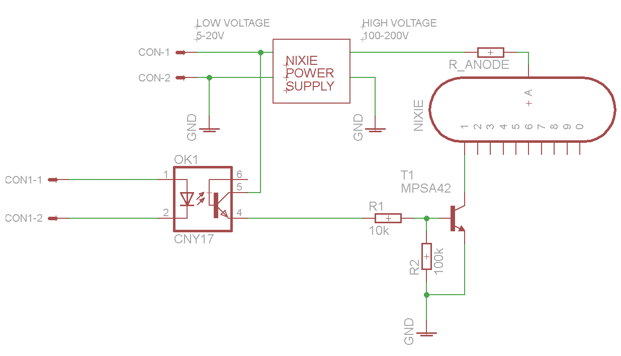
- Safe switching
- Galvanic insulation
- One optocoupler per cathode needed, a bit of overhead
Transistor. Switching cathode indirectly to ground
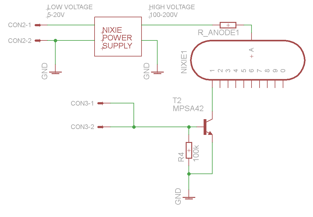
- Indirect switching
- Check Ratio R4 to pullup resistor R1-R16 of first schematic. Should be around R4/R1=10.
- Inverted logic level. In this case cathode is switched on when output is zero!!
Shift Register output FETs: Switching cathode directly to ground with protection.
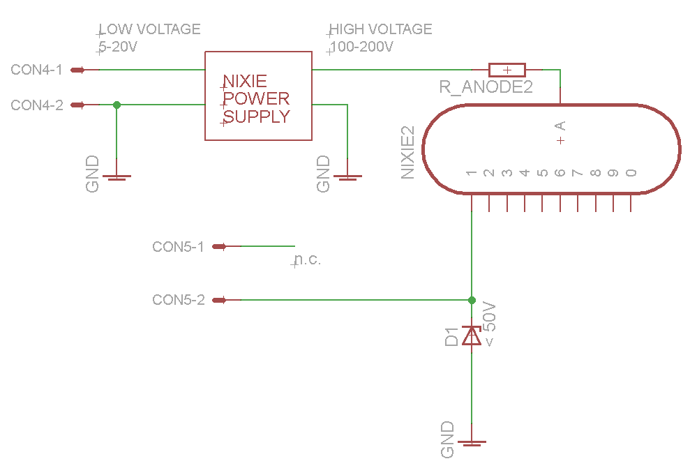
- Cheap, simple
- Out of specification
Last Idea:
if you say, galvanic insulation is a nice idea but you do not want to use so many. What about using the optocouplsers for the shift-register input lines? So the shiftregister is still on the "bad" side but your controller is safe. That's how I would do it if I had more Nixies. Since I only got one and it's more a toy I did not care.
Code
For testing I am using ENERGIA with my Stellaris Launchpad. Same code should compile and run on Arduino. I also encluded delayMicroseconds(1) to ensure timing. Even so it does run without it.
The code displays "0 1 2 3 4 5 6 7 8 9 ." on my nixie in that order. Eventually the order only depends on your wiring ;-)
#define    SEROUT    PA_5
#define    SRCK      PA_4
#define    RCK       PA_3
#define    SRCLR_    PA_2
//#define    G_        IS 0 (GND)

void setup()
{
   pinMode(RED_LED, OUTPUT);
   pinMode(GREEN_LED, OUTPUT);
   pinMode(BLUE_LED, OUTPUT);

   pinMode(SEROUT, OUTPUT);
   pinMode(SRCK, OUTPUT);
   pinMode(RCK, OUTPUT);
   pinMode(SRCLR_, OUTPUT);
   //pinMode(G_, OUTPUT);

   //digitalWrite(G_, LOW);
   digitalWrite(SRCLR_, LOW);
}

void loop()
{
  for(int i = 0; i < 12; i++){
    writeWord((uint16_t)(1 << i));
    delay(200);
  }
}

void clearSR(){
  delayMicroseconds(1);
  digitalWrite(SRCLR_, LOW);
  delayMicroseconds(1);
  digitalWrite(SRCLR_, HIGH);
  delayMicroseconds(1);
}

void trasferSR(){
  delayMicroseconds(1);
  digitalWrite(RCK, HIGH);
  delayMicroseconds(1);
  digitalWrite(RCK, LOW);
  delayMicroseconds(1);
}

void writeWord(uint16_t dataword){
  clearSR();
  for(int i = 0; i < 16; ++i){
    uint16_t databit = (dataword & (0x10000 >> i));
    writeBit(databit);
  }
  trasferSR();
}

void writeBit(uint16_t databit){
  if(!databit)
    digitalWrite(SEROUT, LOW);
  else
    digitalWrite(SEROUT, HIGH);

  delayMicroseconds(1);
  digitalWrite(SRCK, HIGH);
  delayMicroseconds(1);
  digitalWrite(SRCK, LOW);
  delayMicroseconds(1);
}
Finally:
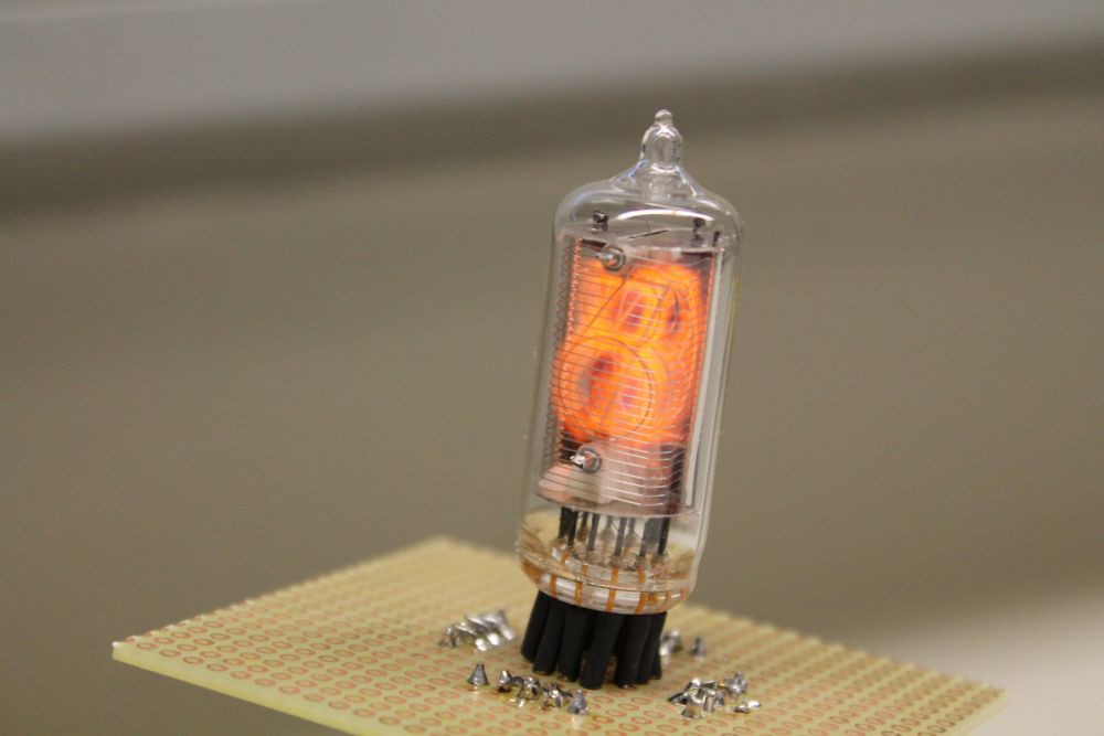
Normal operation:
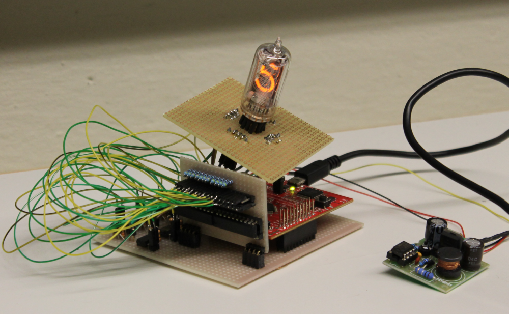
And that's how it lools when you switch numbers with max speed: