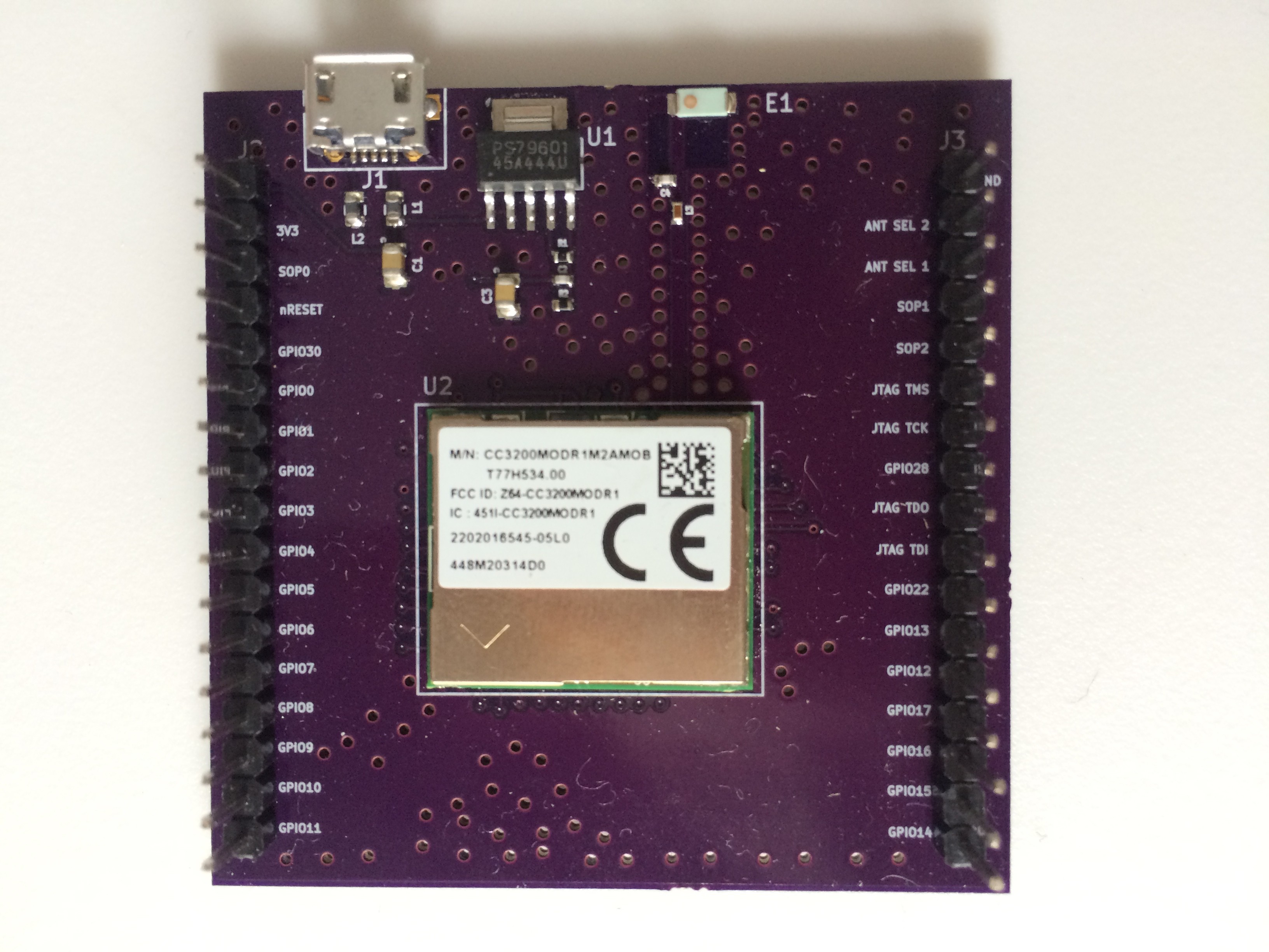
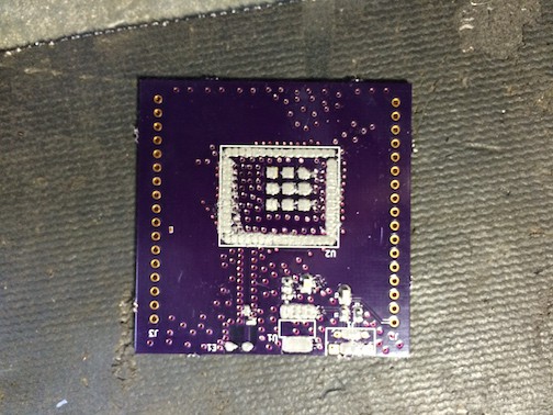
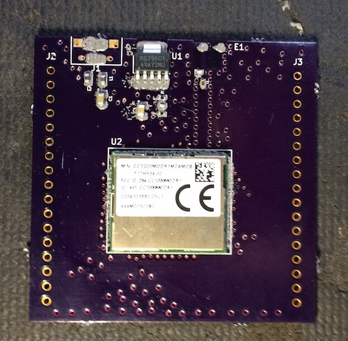
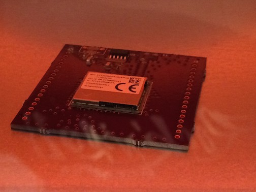
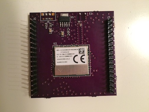
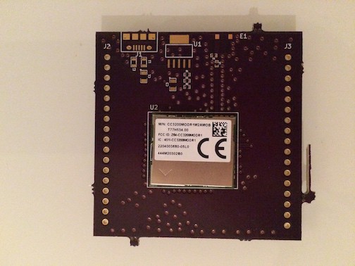
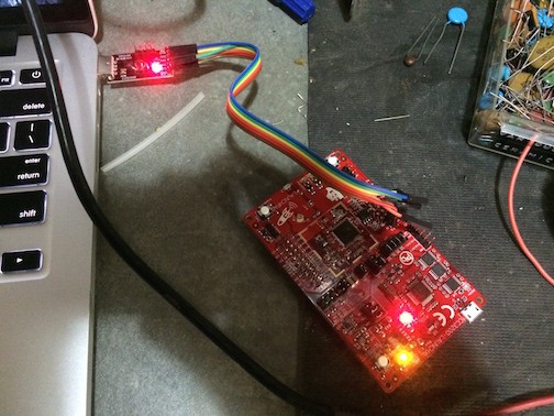
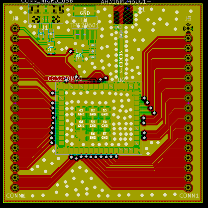
• Assembly, final

    Jackson Keating05/19/2015 at 19:22 0 comments

    I had to give up on hand assembly. I made a few more attempts. However, I could never get it to turn as precisely as necessary. Not to mention, after numerous trips in and out of the toaster oven, I became suspicious that the chip had been compromised. As a result, I turned to the wonderful people at Macrofab, based in Houston, TX. After two weeks of patiently waiting, I received the final product. It worked right out of the box. I spent time testing some basic GPIO and WiFi functionality. Everything worked very well. I have now completed the rough scope of this project.

    Here's a video of the board all wired up and blinking it's first light.

    Next steps will include some simple improvements to make firmware development more easy. Adding a programmer would be a good next step. Improving the form factor to be smaller and more compact. I would also consider adding power LEDs, some GPIO LEDs, and jumpers for the programming pins.

  • Assembly Pt 1

    Jackson Keating03/03/2015 at 03:47 3 comments

    My first attempt at assembling the circuit board was unsuccessful. The LGA package combined with a rushed solder paste application to ruin the first reflow. I tried to salvage the board, but nothing seemed to work. I'll be making a second attempt in the next few days.

    I started off from the ground up. I had never attempted to reflow before so I had to begin with a trip to the store for a shiny, new toaster oven.

    After setting up the toaster oven, I got to work with the stencil. I used OSH Stencils. The stencil lined up really well.

    They're pretty nice, but I'm apparently still pretty bad at using them. The process is a little sloppy. Looking back, I think this may be where I made the biggest mistakes.

    There's lots of extra solder on there. Still, I was in a hurry and didn't know better, so I soldiered on. I got a pair of tweezers and placed the parts on the board. My shaky hands had a hard time placing the 0402 components.

    Watching the components bake.

    The power supply and antenna circuit turned out well, despite the extra solder and small components. But you can see the beginnings of trouble with the small bubbles forming outside the microcontoller package. At this point, I had placed the header pins on the board as well.

    Testing showed spurious voltages on some of the output pins. At that point, I attempted to reflow and remove the extra solder with solder wick. But my attempts to salvage the board failed.

    Overall, I'm going to use more caution assembling the next board. I'm nervous about state of the microcontroller. I've been careful to keep an eye on the parts temperature during testing. I've also done some short circuit testing and nothing appears to be out of place.

  • They're here!

    Jackson Keating02/27/2015 at 12:40 0 comments

    The PCBs came in today. They look fantastic.

    I'll have to wait a couple days to assemble them, but here's a sneak preview.

  • Energia

    Jackson Keating02/25/2015 at 05:37 0 comments

    Spent tonight messing around with Energia. I wanted an easy way to generate some test programs for the incoming PCB.

    Energia is a Arduino based tool for programming TI's series of launchpads. I found it was extremely easy to use. I was up and running in just 10 minutes. I found this tutorial extremely helpful.

    http://energia.nu/pin-maps/guide_cc3200launchpad/

    He goes through two simple tutorials. One blinks a light based on a timer. The other blinks the light based on user controls from a webpage. Everything worked really well.

    I also put the CP2102 programmer through some extra paces. It works well with the Energia IDE. When Energia attempts to enter debug mode after uploading the binary, it fails. Still, the program loads successfully. The serial port monitor also works through the CP2102. I was really happy to find that out.

  • Programming

    Jackson Keating02/24/2015 at 03:50 0 comments

    The boards are on their way! They just shipped out today, which meant that I needed to get started with ironing out the programming procedure. I used my CC3200 launchpad to approximate the incoming CC3200MOD breakout and successfully programmed the chip with an external SiLabs CP2102 programmer.

    After reading the CC3200MOD data sheet, I gathered that it requires a 3.3V UART signal for programming. On the software side, TI provides a programmer, called Uniflash, that supports programming over a COM port at 921600baud. Uniflash has a special version for the CC3200/3100 chips. It can be found here:

    http://www.ti.com/tool/uniflash

    I briefly searched around and found this nice cheap CP2102 breakout board on amazon for about $7. There's several options to choose from, so I just picked a board with good reviews.

    CP2102 Programmer

    A look at the data sheet shows that it is only rated for 1Mbps. At 921,600bps, the TI programmer will be pushing it. The launchpads all use the FTDI FT2232D. They have a higher rated TTL baud rate of 3Mbps and seem to have better support. However, FT2232 breakouts run almost $30. So I went with the CP2102 to see if it would work. I wasn't disappointed.

    Here's the CP2102 programmer I got in the mail

    You can see it's missing some pin headers. Also, from reading comments and looking at the board, you can see that there is not voltage on the Vcc pin.

    After an initial failed attempt, I went to the local hackerspace to troubleshoot. Check out the analog scope

    Here's the programmer hooked up to the launchpad. This is after I took the time to install some pin headers. I also connected Vcc to 5V so that it could power the board on its own.

    I saw that the UART was UARTing, so my attention moved to my setup. Long story short, there were a few issues. I had to switch a few of the launchpad's jumpers. Most importantly, I had the wires all mixed up!

    In the end the programmer worked pretty well. There were a few times where the CP2102 failed on the verification stage. I also saw one instance where it had a bad connection and took a long time to load the MCU image. Still, after a restart, my test program worked exactly as it was supposed to.

    Overall, I'm convinced this setup will work fine with the breakout board that's on its way.

  • Layout week finale

    Jackson Keating02/13/2015 at 07:05 5 comments

    This layout week has ended in success. I just submitted the board to OSH Park.

    After having a majority of the work done last night, this evening was a breeze. That said, I did not review the design. I'm hoping that with a simple board it won't be necessary.

    The last step was submitting the paste layer for the stencil to OSH Stencils. When I was first designing the breakout board I stumbled across a really strange issue. I was trying to size the landing pads for the GND heat sink pins underneath the CC3200MOD. I tried to use the paste layer to size my footprint, but soon found out that the paste layer for the heat sinking GND pins was significantly smaller than the pins themselves. BUT WHY!? Enter The Spark Gap Podcast with their life saving episode on Design for Manufacture (DFM) that I was literally listening to this morning for the first time. Turns out, if there is too much solder paste on these pins, the reflow process can cause the chip to lift off of the PCB and prevent quality connections to the solder paste on the other pins. So, with confidence, I reduced the size of the solder paste layer for those pins specifically. There was so much great information on that episode. I've posted a link if you want to check it out.

    Spark Gap Postcast - 26 - Design for Manufacturing

    Thanks to the podcast I was able to submit to OSH Stencil tonight.

    And there it is. Now I'm just waiting patiently for the parts to come in. This may also be the right time to attempt putting together a programming procedure.

  • Layout week pt 2

    Jackson Keating02/12/2015 at 07:41 0 comments

    Powered through the pour and the via stitching. Never thought about how the number of traces inherent to a breakout board might impact the grounding plane that I need.

    I don't know much about RF. For the sake of speed, I'm trying to rely on the reference designs from TI. Based on the reference design, I tried to maintain a solid ground plane throughout the top layer. At first, I had all of the breakout traces routed on the top layer. This prevented the majority of the board from being filled in by the copper pour. I made the call and moved all of the breakout traces to the bottom layer. This will provide a continuous ground plane for the top layer. Which again. I'm not sure is important at all.

    Stitching with KiCAD is very counterintuitive. Luckily I found this handy video from Contextual Electronics:

    And! It was the first hit in the google search. Made the whole process mostly painless.

    Here's a snapshot of the first draft of the PCB. Barring anything that I remember when I'm less sleep deprived, it should be ready to upload to OSH Park. I'll give myself time to review it tomorrow and hopefully get it out.

    Then it's back to firmware in order to write the programmer code.

  • Layout week pt 1

    Jackson Keating02/12/2015 at 02:17 0 comments

    I'm spending this week laying out the PCB after work. I'm hoping to have a final version submitted to OSH Park in time for the weekend. So far things are going really well. I'm using KiCAD for the first time, so it is a bit of a learning curve on that as well.

    As of last night, I put the finishing touches on the PCB routing to the headers, the power supply, and the antenna. I revised the header net lists constantly for the first few days. I didn't have the foresight to organize them based on the header's proximity to the chip's pins. Then, I forgot to add a header connections for the power and ground because they were already connected directly to the chip.

    The antenna required some thought. The launchpad design (aka the design that I am liberally ripping off) has a smooth bending route from the antenna to the pin. Apparently, RF signals do not do well with 45° bends. I struggled trying to get KiCAD to do the same thing. Turns out, this is impossible. Finally, common sense kicked in and I had the idea of placing the antenna so that I could create a straight route to the pin. Voila.

    Without any major hiccups, I'm well on my way to ordering the first draft. Next up is the fill and copout areas.