 Bud Bennett
This project arose because an engineering friend asked the question, "How does this compare to the competition?" I responded that it would be much easier and cheaper to just build a magnetic switch without any of the battery backup aspects. So here it is.
Power to the load can be switched on or off by momentarily placing a magnet near the circuit. This allows the circuit to be completely enclosed within the aircraft fuselage. The current drawn from the batteries while in the off-state mode should be as low as possible. It should take more than one year to discharge the battery. The voltage drop across the switches should be as low as possible to keep power dissipation, heat, and losses to a minimum.
The twist on this application is that it should remember the state of the switch if the input power is disrupted or disconnected for up to 10 seconds. It would be disastrous if the power glitched during a flight and the switch permanently disconnected all of the electronics controlling the operation of the aircraft.
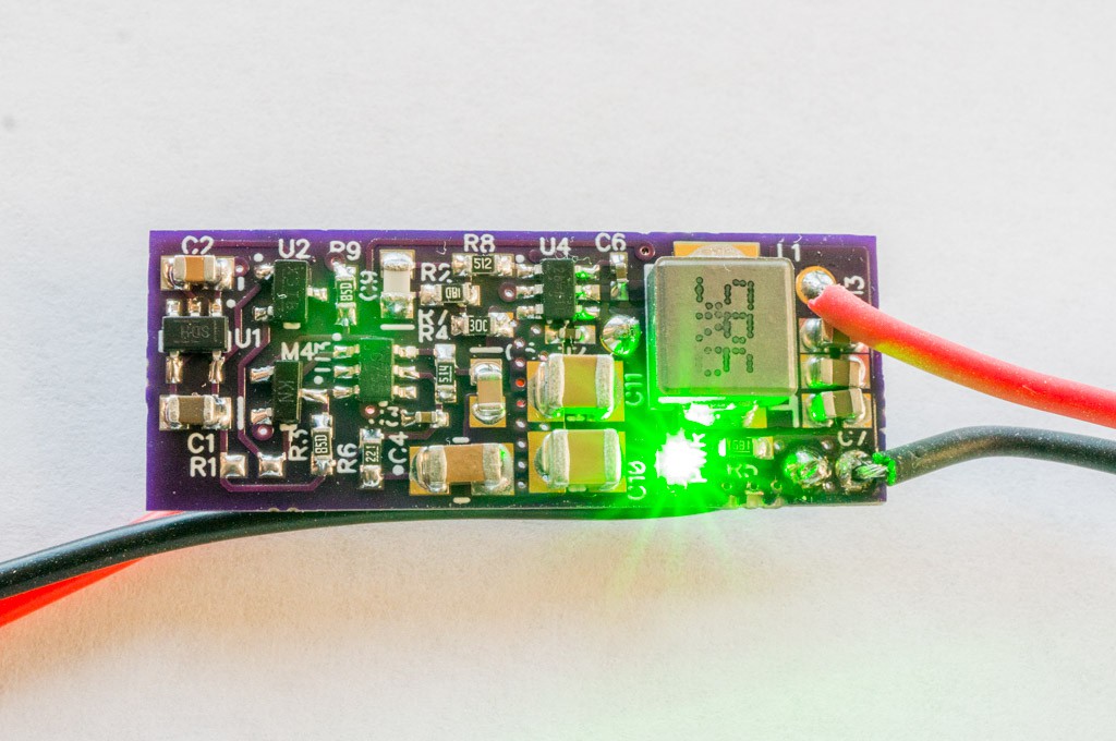
I've decided to pursue four types of switches. One for low current/low voltage applications such as RC gliders without motors. Two with higher current and voltage for motorized RC aircraft. A fourth with an integrated battery eliminator circuit (BEC).
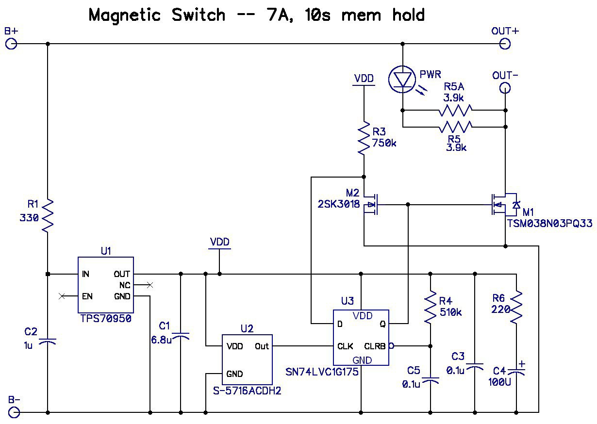
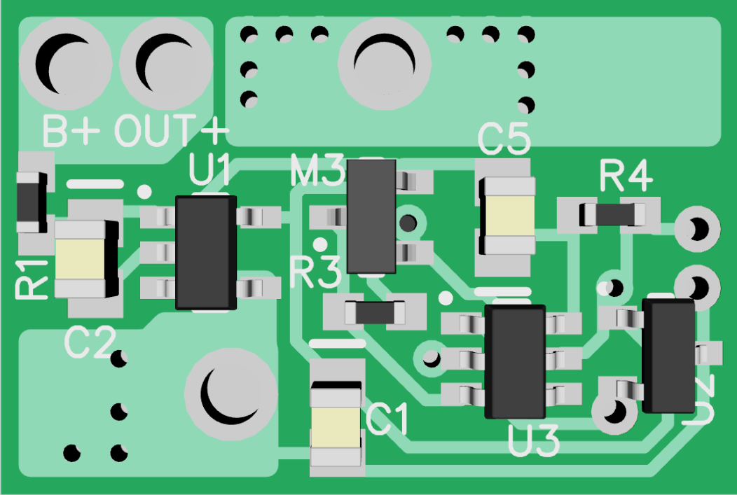
Low Current Switch Specs:
Input Voltage Range: 3 - 30V (1S to 6S LiPo/Li-Ion battery)
Max current to load: 7A continuous, 10A for <30 seconds
Insertion Loss across switch at 7A: < 30mV
Off-state Current: 5µA
On-state Current: < 15mA
Power State Memory Hold Time: > 10 seconds
Size: ~ 10 x 18mm (smaller is better)
Cost: ~$3.75
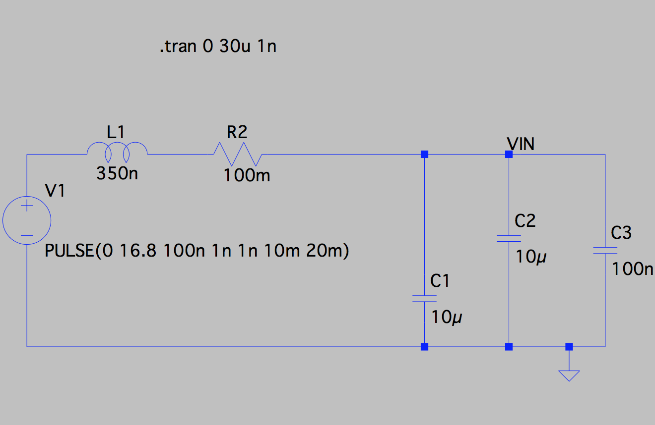
Latest Schematic (2018-03-28):
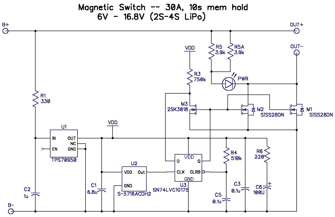
4S/30A Switch Specs:
Input Voltage Range: 6 - 20V (2S to 4S LiPo/Li-Ion battery)
Max current to load: 30-40A
Insertion Loss across switch at 30A: <40mV
Off-state Current: 5µA
On-state Current: < 15mA
Power State Memory Hold Time: > 10 seconds
Size: 13.3 x 20mm
Cost: ~$5.33
Latest Schematic (2018-03-28):
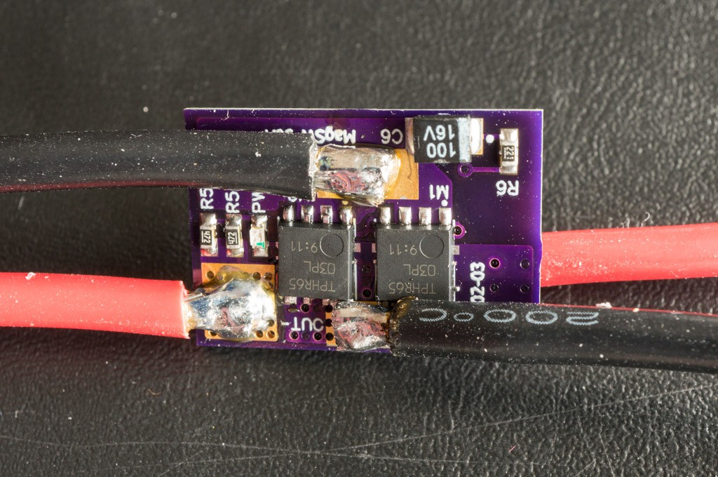
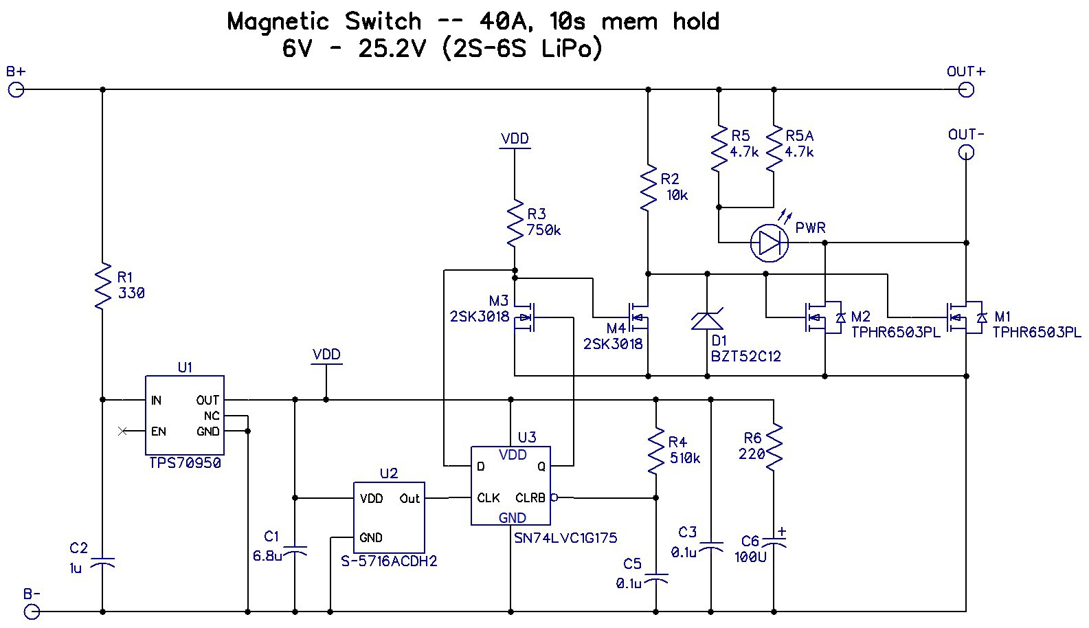
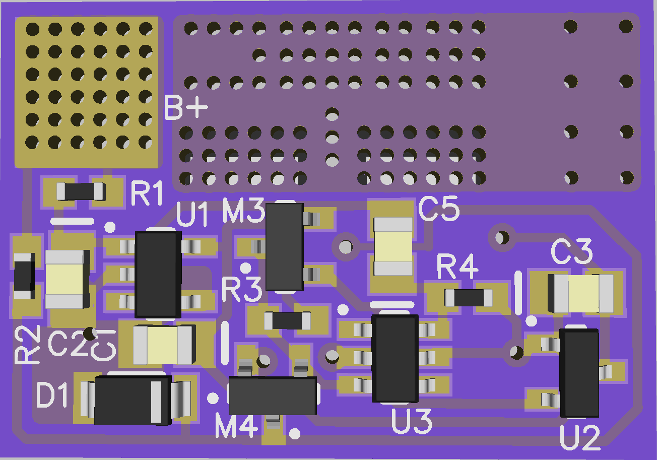
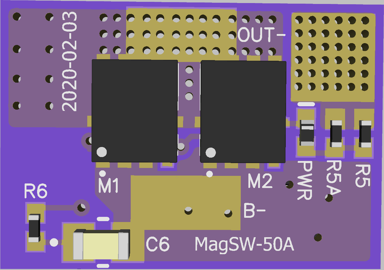
6S/50A Switch Specs:
Input Voltage Range: 6 - 30V (2S to 6S LiPo/Li-Ion battery)
Max current to load: 50A
Insertion Loss across switch at 50A: <20mV
Off-state Current: 35µA @ 12.6V, 50µA @ 25.2V
On-state Current: < 10mA
Power State Memory Hold Time: > 10 seconds
Size: 16 x 22.7mm
Cost: ~$TBD
Latest Schematic (2020-02-02):

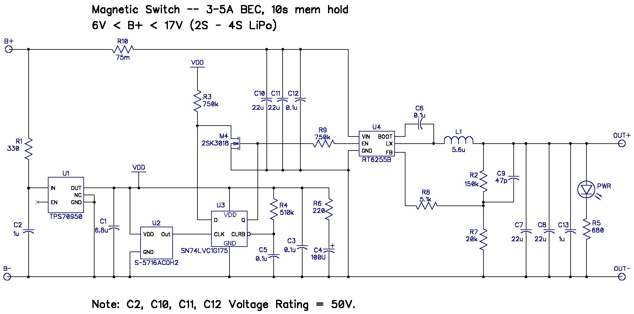
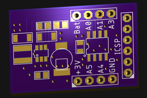
Switch + BEC Specs:
Input Voltage Range: 6 - 18V (2S to 4S LiPo/Li-Ion battery)
Output Voltage: 5V ± 5%
Max continuous current to load: 3A or 5A versions.
Max burst current to load: 5A or 6A versions.
Efficiency: >90% at max load. (500kHz switcher)
Off-state Current: 10µA
Power State Memory Hold Time: > 10 seconds
Size: 13 x 35mm
Cost: ~$6.00
Latest Schematic (2018-03-28):


 Ted Yapo
 David Scholten
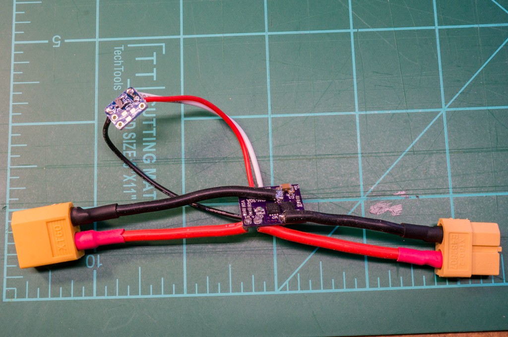
This is really awesome! Thank you for sharing! I am going to try the low current switch design in my L2 rocket build to turn on the altimeter! I am trying to get my head around the design, does this handle reverse polarity?