 Open Green Energy
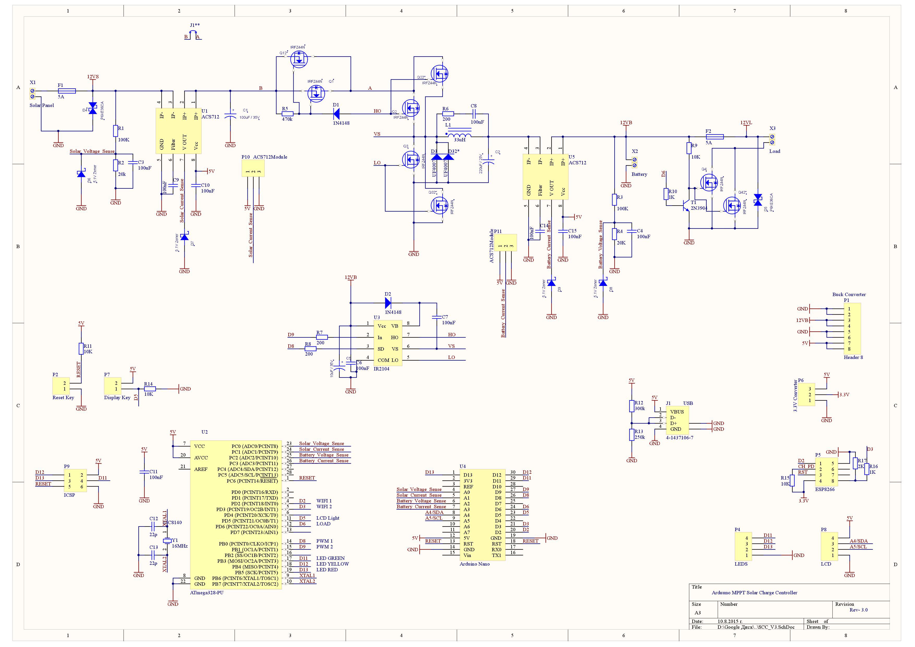
For easier prototyping I decided to make a PCB for V-3 Charge Controller.To make the PCB more versatile, the schematic has been modified on 21 th June 2015.The schematic has been drawn in Altium PCB designing software by Petar. These are the following modification in the updated schematic.
1. Improvident of voltage sensors :
The voltage sensors out put is directly hooked up to the Arduino Analog pins A0 and A2. Any unwanted surge may damage the analog pins.So to protect from these surges 5.1V zener diodes ( D6 and D8 ) are included.
2.Adding space for ACS712 chip on PCB :
Though ACS712 module is used now, we left space for ACS712 smd chip along with its circuitry on the board.The smd ACS712 chip is cheaper in compare to the ACS712 module.So it will be helpful in future.
3. Adding one more parallel MOSFET in the position of Q1,Q2,Q3 and Q4 :
To handle more power in future, there may be need some extra MOSFET to fulfil the current requirement.So additional MOSFETs are placed in parallel to the Q1,Q2,Q3 and Q4.The new MOSFETS are Q12*,Q22*,Q33* and Q44*.
4. Adding a additional diode parallel to D3 in the buck converter circuit.The new diode is D32*.
5. Space for Atmega328P : Added space for Atmega328P along with Arduino Nano board.So user can use according to his choice.The on board Atmega328P option will reduce the power consumption as well as cost.
6. Programming Port for Atmega 328P :To program the Atmega328P directly, ICSP port ( P9 ) is provided.
7.USB port is placed on board.Two additional resistors ( R12 and R13) are used for enhancement in the USB circuit.
8. Adding one more current sensor ( ACS712 ) : To monitor the battery charging current.
PORT description :
P1 : Buck Converter Module
P2: Reset Key
P4 : LEDs
P5 : ESP8266
P6 : AMS1117 module
P7 : LCD back light Control Key
P8: I2C LCD connection
P9: ICSP programmer
P10: ACS712 out put to monitor solar panel current
P11: ACS712 out put to monitor the Charging Current.
Discussions
Become a Hackaday.io Member
Create an account to leave a comment. Already have an account? Log In.
My own hard learnt lessons:
Your 5.1V zener diode might draw a small amount of current well before it gets near 5.1V. That current will affect the reading of your voltages from the voltage divider. Given that you have a 100K series resistor, it doesn't take a lot of current to introduce enough I*R drop to affect your ADC reading.
One way is to pre-bias the zener diode and use a switching diode in series to clamp the signal(s) as the switching diode has very low leakage current. The quick fix is not populate the zener and simply relies on the 100K to limit the input current.
Also want to make sure that C4 is located as close as possible to your ADC input pin as the signal from the divider has high impedance. I have seen a difference on my old charger layout when the 0.5" track between the cap and the ADC input introduces random reading.
Might also want to look into putting the foot prints for a small series resistor on each of the MOSFET gates. Sometimes there are high frequency rings for driving large banks of MOSFET. Use a zero ohm for now and if you ever run into EMC or other troubles, you can easily swap in a small value (a few ohms) to slow down the slew rates. The resistor also help to damp out high frequency oscillation due to parasitics (track inductance, gate capacitance etc).
Are you sure? yes | no
Thank you Lee for your valuable suggestions. I appreciate it.
Are you sure? yes | no