 Hacker404
It'll be easy they said!
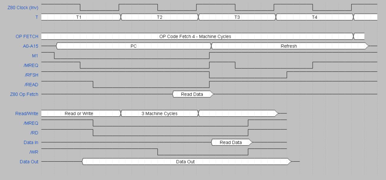
I spent many hours using WaveDrom as a visualising tool for the timing. At the end of this many hours, I decided to split the diagram into several parts. I discovered that the "Save As" function does not change the default file name so the original file is overwritten when you close WaveDrom!!! Much frustration. I lost everything except the above.
Anyway this CPU is *not* the easiest chip to bus time share with. As you can see from the Op-Code fetch above, it wants the Address bus just about all the time.
It also has two different SRAM Read timings, one for op-code fetch and another for normal access.
One other notable feature is the very wide data out write window.
There is also one other 'problem': I want to be able to write to the FLASH (ROM) from the CPU. I will mention what is a problem with that later.
Here's what I came up with and they're just thoughts now that I have lost the diagrams that I made.
Because of the two different read cycles and data in windows, I will buffer reads to a local register (in the CPLD) so the CPU can grab the data when it is ready. Even though the read data-in windows are completely different, the control signals /MREQ /RD start off almost exactly the same way. Each T cycle will be divided up into 3,4 or 6 sections and the read will happen the earliest and read later by the CPU when it is ready.
A Write (to RAM or FLASH) won't need buffering as the data out window is so long. There is one problem though. The write control window is longer than one T cycle. This means a second write to the same location may occur. If this were to happen then the CPU couldn't write to FLASH as it has 'write protection' that requires a specific sequence if write to effect one byte update.
So in total - there should be at least 4 time slots -
1) CPU Read - RAM or FLASH
2) Graphics Read - RAM (Character ASCII number)
3) Graphics READ - FLASH (Character Pixel map - one line)
4) CPU Write - RAM or FLASH
There will be 6 CPU T cycles to one screen character.
The screen dot clock will run at 25 MHz
The CPU clock will be 2.083 MHz
Now I have to make sub timing diagrams for these processes and then I can write it to HDL.
These timing windows won't actually fit together so I will also buffer the data for pixels and have it one character late so they transfer at the very start of the next T cycle. This will mean I have to adjust the Graphics timing to pre-compensate for this.
OK, next step is to go and redo and finish the timing diagrams that I lost.
One drawback that is likely from all of this is that each unit will most probably have to be programmed specificity for the video standard it uses: PAL, NTSC, VGA, because all of these standards are not going to fit in a CPLD together.
Discussions
Become a Hackaday.io Member
Create an account to leave a comment. Already have an account? Log In.