 Michel Kuenemann
Main features of the LPC1102
- ARM Cortex-M0 based processor
- 32-bit MCU
- CPU frequency up to 50 MHz
- 32 kB on-chip flash memory
- 8 kB SRAM
- 11 General purpose input output pins
- 10 bit ADC
- 1 UART
- 1 SPI controller
- Internal 12 MHz RC oscillator
- Consumption: approx 2 mA @ 12 MHz
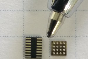
- Package: Wafer level chip-size package, 16 bumps, 2.17 X 2.32 X 0.6 mm
This device is currently one of the smallest Cortex M0 based processors available on the market.
Aspect and pinout of the YoctoBob module
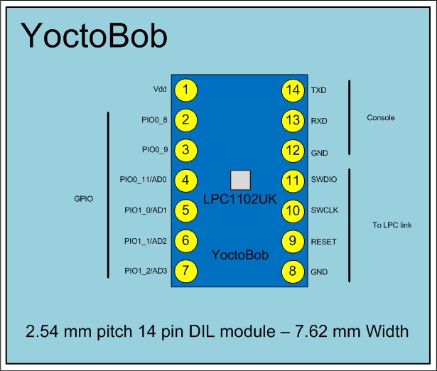
(Pinout updated on 2015/05/24)
MCU pin allocation
| Bump | Pin designation | YoctoBob Pin number | YoctoBob Pin designation | Remark |
| D2 | VDD | 1 | VDD | Power Supply |
| A2 | PIO0_8/MISO/CT16B0_MAT0 | 2 | PIO0_8 | GPIO |
| A3 | PIO0_9/MOSI/CT16B0_MAT1 | 3 | PIO0_9 | GPIO |
| B4 | R/PIO0_11/AD0/CT32B0_MAT3 | 4 | PIO0_11/AD0 | GPIO |
| B3 | R/PIO1_0/AD1/CT32B1_CAP0 | 5 | PIO1_0/AD1 | GPIO |
| C4 | R/PIO1_1/AD2/CT32B1_MAT0 | 6 | PIO1_1/AD2 | GPIO |
| C3 | R/PIO1_2/AD3/CT32B1_MAT1 | 7 | PIO1_2/AD3 | GPIO |
| D3 | VSS | 8 | GND | Power Supply |
| C1 | RESET/PIO0_0 | 9 | RESET | Programmation |
| A4 | SWCLK/PIO0_10/SCK/CT16B0_MAT2 | 10 | SWCLK | Programmation |
| D4 | SWDIO/PIO1_3/AD4/CT32B1_MAT2 | 11 | SWDIO | Programmation |
| B1 | VSS | 12 | GND | Power Supply |
| C2 | PIO1_6/RXD/CT32B0_MAT0 | 13 | RXD | Console |
| D1 | PIO1_7/TXD/CT32B0_MAT1 | 14 | TXD | Console |
| A1 | VDD | N/A | ||
| B2 | XTALIN | N/A |
(Table added on 2015/05/17)


 Andy
Andy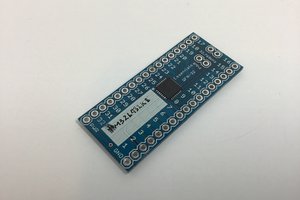
 Ben Lim
Do i see via directly in the BGA pad? This is a big no-no IMHO, they'll suck the solder righ in the hole and you won't have a good contact between the ic and the pad or not at all. Unless you plan to do fully copper filled via?