0%
0%
Bipolar dudes
A group for those who want to build their own bipolar transistors
 Yann Guidon / YGDES
Become a Hackaday.io member
Already have an account? Log in.
Just one more thing
To make the experience fit your profile, pick a username and tell us what interests you.
Pick an awesome username
hackaday.io/
Your profile's URL: hackaday.io/username. Max 25 alphanumeric characters.
Pick a few interests
Projects that share your interests
People that share your interests


 Matt Moses
 Michael Barton-Sweeney
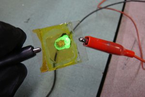
 Ian Hanschen
 Brainy.Baboon
https://www.youtube.com/watch?v=5x6Ob3EYkcg Thank you Fran Blanche :-)