 drewrisinger
High quality sound should be a right, not a luxury. To that end, I worked to make a cheaper, open-source version of cobaltmute's pupDAC for a EE PCB design class.
Over the course of a semester, we selected a circuit, analyzed it, turned it into a MultiSim schematic, turned that schematic into a board layout , and then ordered and built the board. I knew that it would be a challenge to build this board, as I was targeting a very small footprint (2"x3" for 80 components) and a relatively complicated design, especially for my first board layout ever.
Soldering Challenges
The following video shows a timelapse of me constructing the board, which required great soldering dexterity.
For my board, I started with a solder paste mask, and spread solder paste over the top surface (0:01). Then I used tweezers to place the parts, and stuck it into a reflow oven. Here, I discovered that our school's default temperature profile was inadequate for my board, because it essentially flash-flowed the oven. It didn't have a soak time, which meant that the ground plane didn't have enough time to heat up, and any parts connected to the ground plane (like all my capacitors) needed manual soldering to melt the paste.
Even with this complication, It would've been a simple job, except that I ran into a nasty problem after I had already started assembling the board: the main IC, a USB to I2S audio data converter, was too large for the footprint (I later traced the error to MultiSim having a too-small footprint for the TQFP-32 package).
So, like any enterprising student whose grade relies on his circuit working, I decided to take the logical next step: solder jumper wires directly from the pads to the leads of the IC (no, I couldn't have ordered a new board, I only had a week till the semester ended, and I still had to redesign the board).
Even though both my professor and our lab technician recommended against this jumper idea, I decided to carry on with my audacious plan. I initially thought I could find some 8-wide ribbon cable, and solder that to the pads, and then fan that out to the IC itself. However, the insulation was too wide, and I couldn't get the leads to stay well-joined to the pads. At this point, I should probably note that the leads of a TQFP-32 are spaced .8mm apart, and the pad that I was soldering onto was spaced at .5mm apart. The next step was to get some wire wrap from the school's technician, which was between 30-32 gauge, and JUST BARELY fit onto the pads (I believe they are 10 mil pads).
I couldn't find wire strippers that worked for wire that small, and using my teeth was ineffective (I ended up bending the wire more than stripping it). So I figured out a way of stripping the wire that was more effective than any other method I found yet, with a yield of maybe 50%... I used a knife to cut the wire to length (roughly 1/4"). Then I would roll the wire under the blade while applying very light pressure. Half of the time, this would create enough of an edge for me to pull the insulation off with a fingernail (the other half it would just cut straight through the wire, and I'd start over). This can be seen at 1:08 in the video.
After making the 32 jumpers needed to connect the IC to the pads (and a few extras for the inevitable problems. And then a few more...), I got down to the slow and touchy process of actually soldering them to the pads (0:47). After getting them onto the pads (1:17, a process that wasn't totally included in the video), I then had to somehow carefully bend the fragile fragile wires up (without breaking them or tearing them off the board), and then solder the IC onto them without heating them too much that the pad end of the wire would come loose. Which happened more times than I would care to admit...
Once I found a rhythm, it was fairly easy to get going, but I still ran into some problems. One was the above-mentioned wires coming loose. If the wire was on the end of a set of 8, it was no problem. I'd just put a new one...
Read more »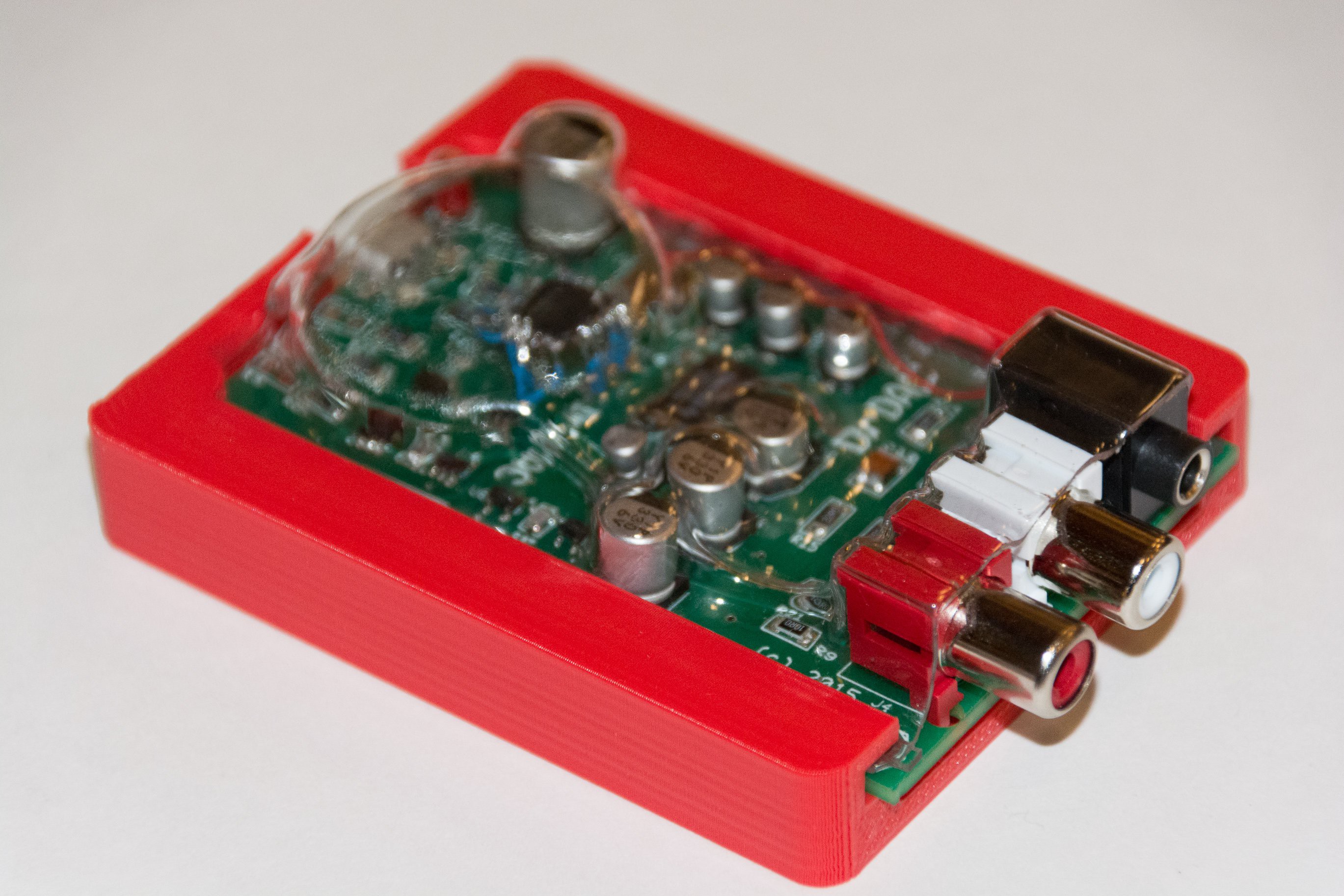


 Skyhawkson
 Koen van Vliet
 Jeremy Gilbert
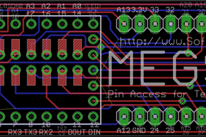
 T. B. Trzepacz
I use regular 0,2 mm enamelled copper wire for patches on boards. if you heat up the bare end of the wire and add some solder, the enamel will just burn away. My methode would be to make a amount of wires all the same length and tin the ends. then solder the wires flat onto the pcb and bend them in a curve back up. A very sharp tweaser is a must. I can dot his with a regular weller wtcp with the sharpest point available. Oh and tinning the pins of the tqfp beforehand also helps.