 David
DavidOne of the 2015 Hackaday Prize criteria is "“Wow” factor: is the entry innovative, is the build impressive?" Well, aside from the "Wow" of a DNA-based molecular diagnostic device, I hope this entry log is a little bit 'wow' on the build side too :)
PCB boards, stat!
Having got my (hopefully!) final schematic and PCB layout finalized, today it was time to fabricate my first PCB. Luckily, if I have messed it up, I can make new versions quickly using this technique :)
Board Preparation
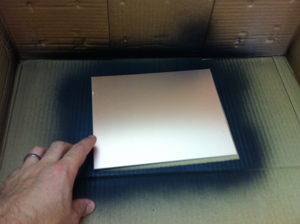
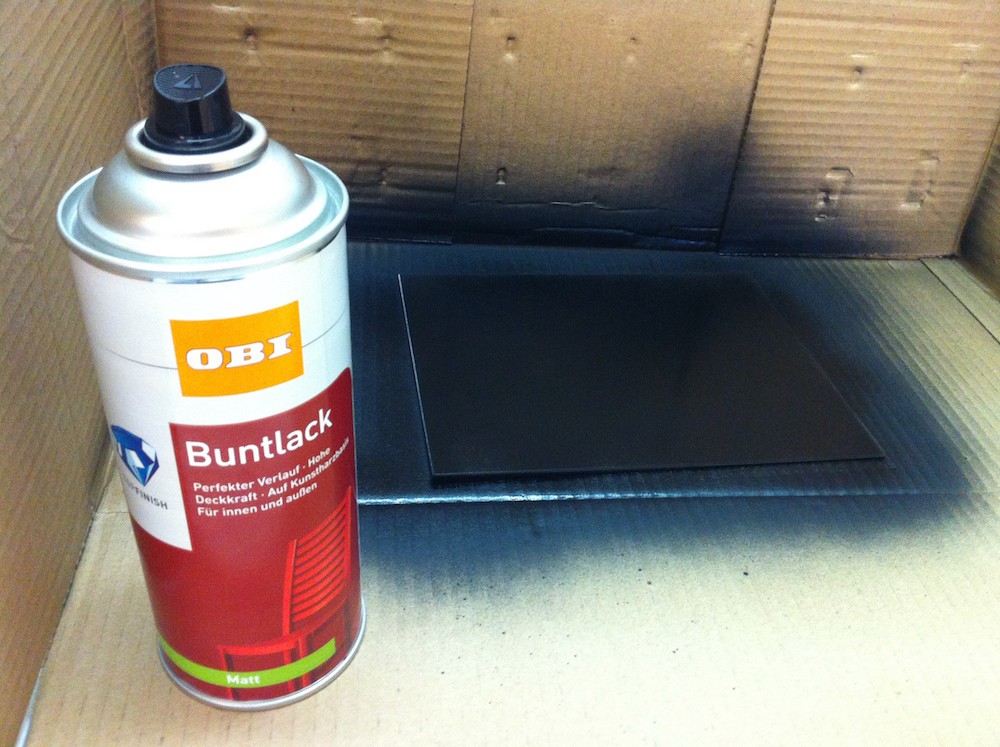
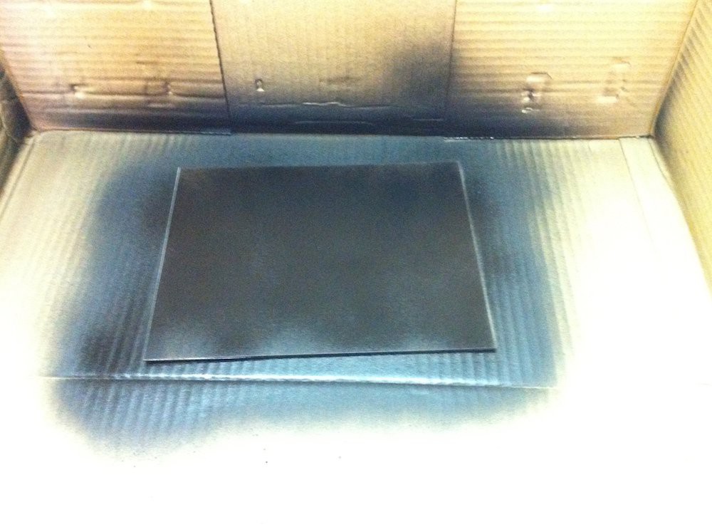
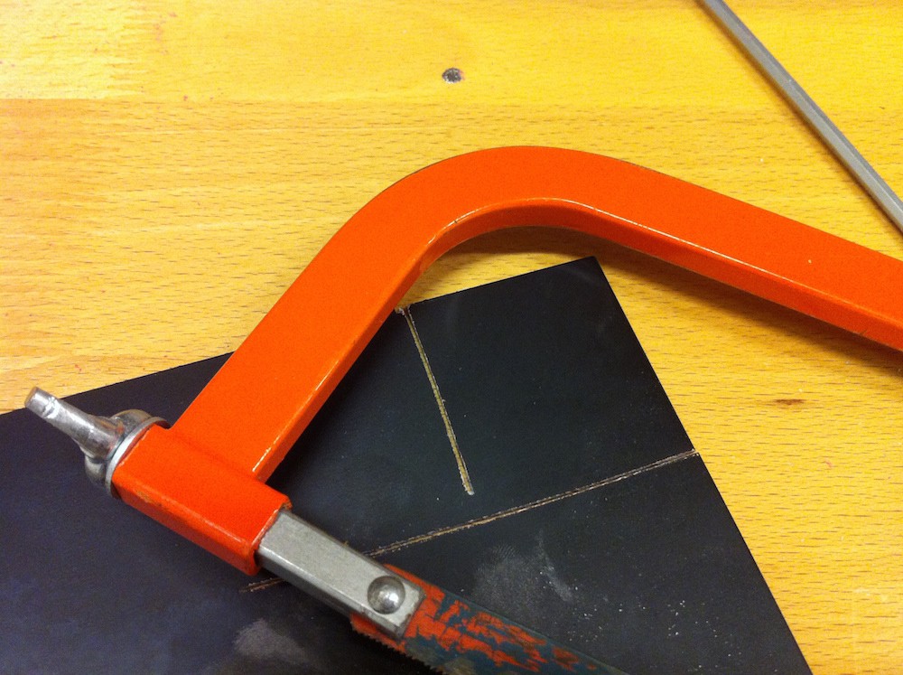
I used off-the-shelf single sided copper board. I gave them a light coat of black spray paint, waited 5 minutes, and a second light coat covered the copper I missed on the first pass. After 10 minutes, the boards were touch dry, and ready to use. I used a hacksaw to roughly cut out a section of board the right size for my design.
 |  |
 |  |
File Preparation
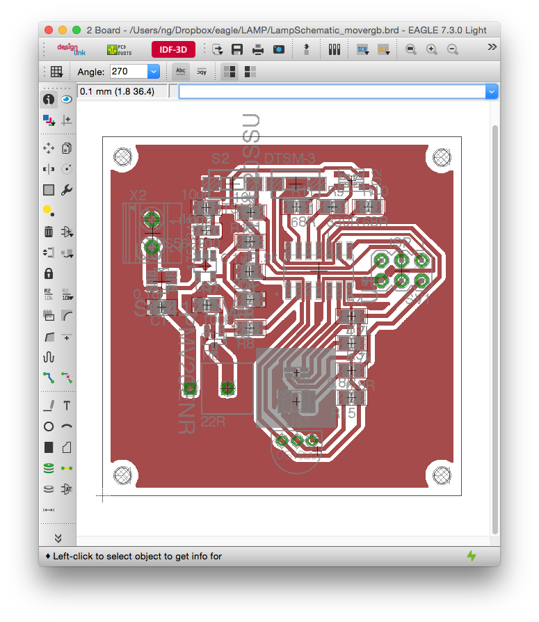
During the drying time, I prepared my PCB files. My board layout has the interface at the top, consisting of a reset and run button, and a RGB status LED. In the middle is the power input on the left, microcontroller in the middle and ISP programming port on the right. At the bottom is the heater, and the sample chamber location, marked by the grey square. Under it is the RGB sensor and UV excitation source for the fluorescent dye.
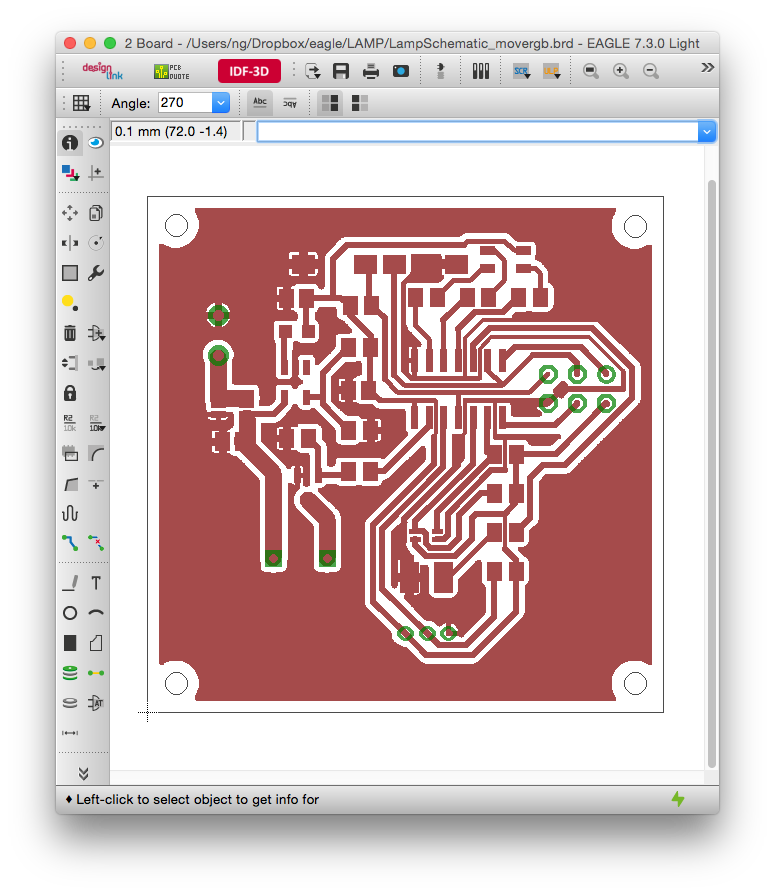
Making a PCB quickly requires just a few steps. The first is to hide all layer that should not be etched. I hide everything except for the top layer, pads and the dimension layer.
 |  |
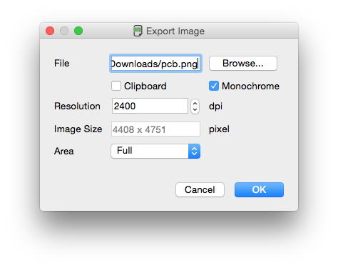
Then, I exported the image, at the highest resolution of 2400 DPI, and set the export to Monochrome. After that, use any graphics program to invert the black and white image, and you are ready to laser your boards.
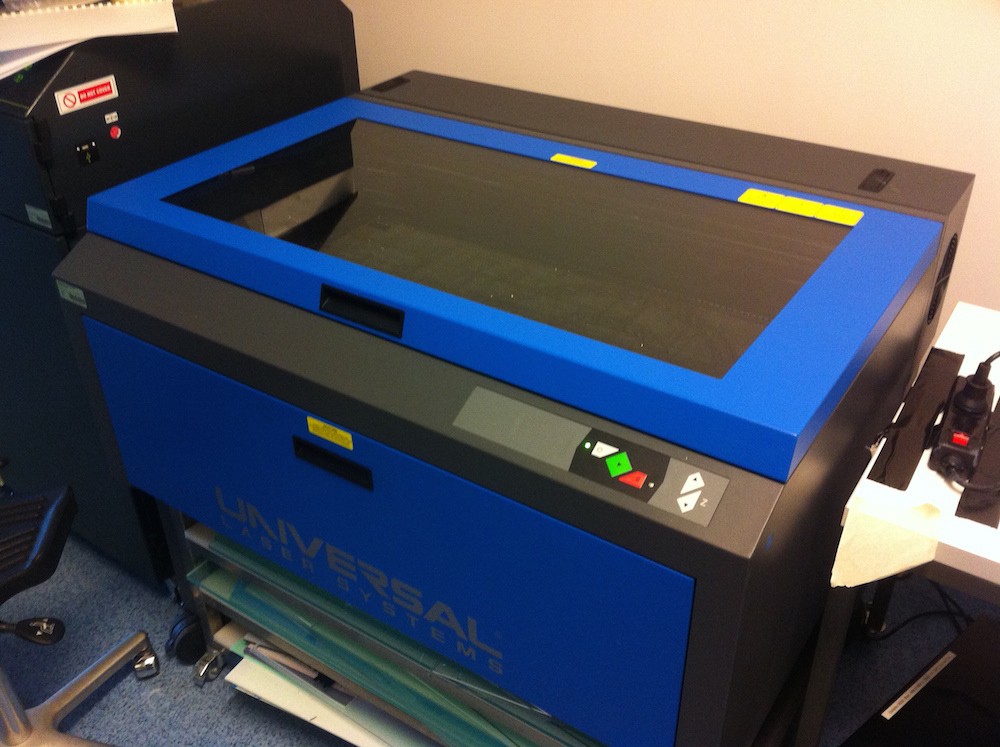
Laser Engraving
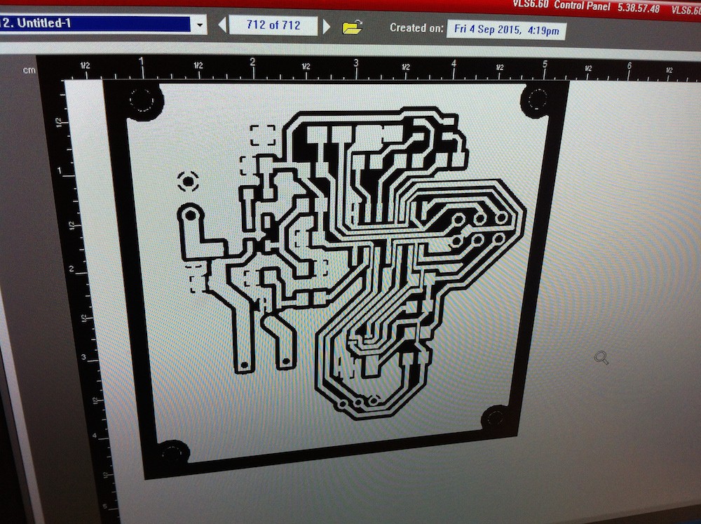
Like most CO2 laser cutters, the one I used has an "engraving mode", that can mark acrylic, anodized aluminium and wood etc. with a black and white image. A quick test found that the engraving settings for acrylic were perfect for ablating the spray paint from the copper surface, allowing the exposed copper to be etched in the next step. It's import to mention that you can't cut the copper laser directly with a regular CO2 laser system. You can do it with a expensive pulsed laser system, but you won't find one of those at your local Hacker Space. Anyway, you just place your painted PCB in the machine, load up the files with the settings for acrylic engraving, and you have your mask ready in about 3 minutes!
 |  |
 |  |
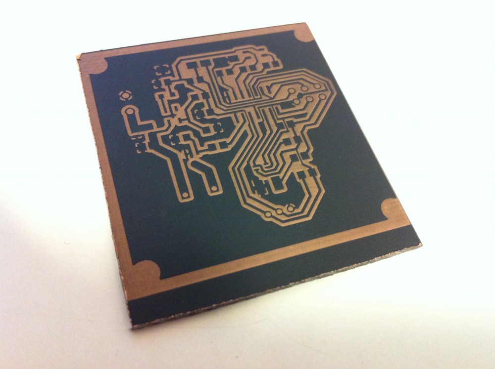
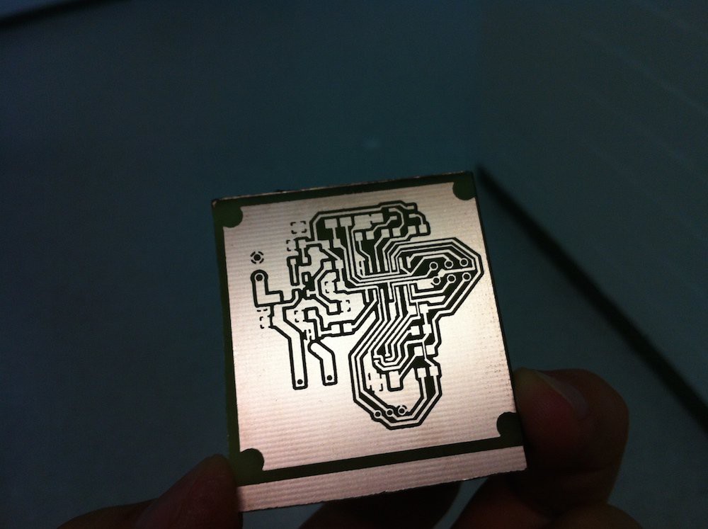
PCB Etching
After that, you do a regular PCB etching. I used a Ferric Chloride bath using the regular method you can find on google, and then removed the black spray paint mask with some solvent. Acetone removed spray paint very easily, so you won't need more than a few millilitres on some tissue paper. A quick soak and wipe, and you are finished!
 |  |
 |  |

If you have a few painted copper boards ready, you can go from the designs on your computer to a physical PCB board in about 5 minutes more than your etching time!
Discussions
Become a Hackaday.io Member
Create an account to leave a comment. Already have an account? Log In.
Have you thought about or tried using this process to also make the soldermask for the boards?
Are you sure? yes | no
If you can suggest a solder mask material, I'll definitely try it out.
Are you sure? yes | no
I think he meant using black spray paint as well?
Are you sure? yes | no
Yes, I was thinking of trying the same spray paint you used for the etching mask, just for the sake of simplicity. Obviously ordinary spray paint doesn't have the same properties as proper solder mask, like resistance to heat and repelling solder, and it's not even a cost advantage (e.g. to the stuff used here http://hackaday.com/2012/09/10/put-a-solder-mask-on-those-homebrew-pcbs/) but I'm curious if it would work anyway. I'm asking because I once soldered a nut to a thin sheet of metal with a gas burner (soldering iron took too long) and the acrylic spray paint on the other side got destroyed by the heat but I think at regular soldering temperatures the paint might stay intact and work as protective layer.
Alternatively you could try solder mask as used in the link above. In this case I'd be curious if the laser can ablate the solder mask in it's dried+uncured form and/or after curing, which would eliminate the photolithography step required otherwise.
Using the spray paint also as protective layer and therefore requiring one less material (liquid tin/proper solder mask) seems to be the only advantage of this idea... maybe with the exception of possibly also using other colored paint ;)
Btw: Did you tin the board after etching? From the images it's a little hard to tell because in one it looks silver colored and in the next it still looks like copper.
Are you sure? yes | no
I hadn't even considered using black spray paint, as I doubt it would survive the soldering temperatures and probably burn and release toxic smoke.
I will give it a go next week though. What might work nicely is something like this:
http://www.net4sale.com/Shop/pc/viewPrd.asp?idproduct=127
It's a clear coat high heat automotive spray paint, rated to 650 Celcius. This particular company also sells a nice green version too :)
Lastly, no, I didn't tin the copper. It's just lighting effects.
Are you sure? yes | no
Hi David, in case you're interested, I did a quick and (very) dirty test to see how the spray paint I have on hand holds up against soldering temperatures: https://hackaday.io/page/1212
I don't think there's a huge difference between spray paints so I'm very much looking forward to your test :)
Are you sure? yes | no