 PCB designer
Etching
DIY PCB by etching is probably the most common way of creating circuit boards by hobbyists. Even though more and more people are opening their eyes to the sweet world of cheap PCB prototyping using fab-houses.
Many versions of this process exists. It can be a bit of a hassle with all the chemicals and equipment. And vias are a pain-in-the-butt. But if you need to test a design fast, then etching is the way to go. I don’t have this kind of equipment at home, but the hackerspace I’m a member of has it.
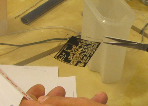
An overview of how to etchPrint your board layout on a sheet of transparent paper:
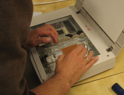
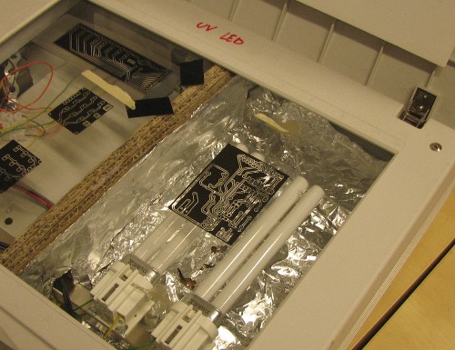
Transfer the layout to the board (Using UV light):
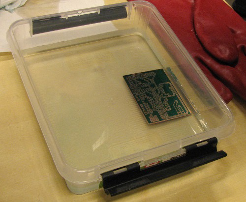
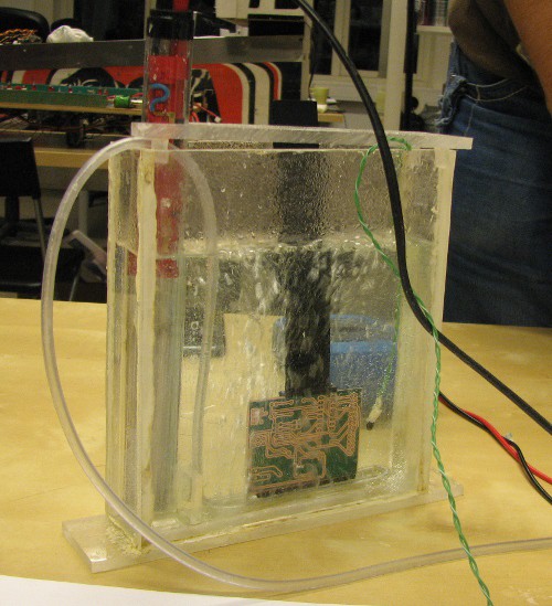
Put the board in an etching solution:
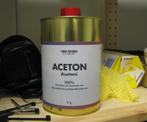
Clean the board with Aceton:
CNC mill
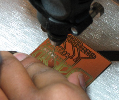
A CNC mill is a machine that mills off the unwanted copper of your
board. When I went to the University of Oslo we had access to a CNC
mill. It was great to be able to mill a PCB, but placing vias manually
is a real pain-in-the-butt if you have a lot of them.
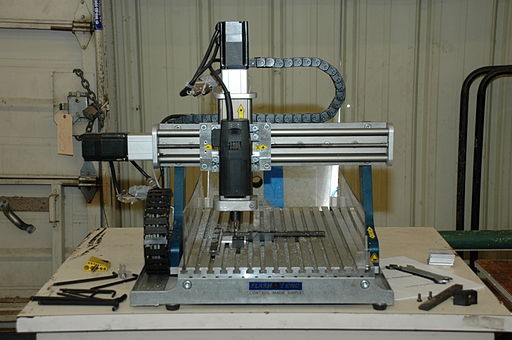 CNC mills can be very expensive, but I have also seen many DIY projects where people build their own mills.
Fab house
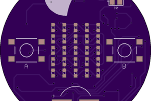
This is my favorite option and I use it all the time. The process goes like this:
- Design your PCB using some PCB Software
- Create Gerber files
- Send your Gerber files to a prototype manufacturer
Okay, you have to wait a bit longer than the two above options, but you can make really complex circuits and you can be pretty sure that if something doesn’t work it’s probably because you have done a mistake either in the schematics/board layout or with your soldering
 Alexander Ryzhkov
 Benchoff
 Michael Delaney