 Ian Hanschen
Featured on HaD, 03/06/2014.

Ever since I saw a YDPG18A mod post where flash was upgraded (unsuccessfully), I’ve been curious about upgrading NAND flash. After I started investigating I realized the upgrade mentioned wouldn’t work, so I called the guy on it and he mentioned it didn’t work, just that he hadn’t gotten around to posting about it. If he’d found the exact same model flash chip as the existing one, soldered it on, and reflashed, it would have worked. But a lot of the flash chips used in these devices are old and hard to get ahold of. Luckily, they use a standard footprint (TSOP48), and a standard pinout used for SLC and MLC NAND flash.
When a system is flashed using LiveSuit, LiveSuit first sends over some modules located within the flash image file to load into system memory to assist with the flashing. One of these modules partitions and formats the NAND flash – then individual blobs of data are sent for each partition. The thing about these flash chips is that even though they often come in a TSOP48 package, they all have different model numbers, which can be queried from the chip. They also have different geometry – number of dies in one chip, number of sectors, number of blocks, and page size. The driver only supports the same model of flash for every flash chip the board is populated with – otherwise it will ignore everything but the first chip.
AllWinner has a generic NAND flash driver which is compiled into Android, the bootloader’s sprite.axf and U-Boot (on 4.x devices), the generic ‘boot’ image that jumps to the bootloader, and the binaries that LiveSuit sends over to assist with flashing the device during a flash. This generic driver contains several tables, one for each vendor of NAND supported, containing each supported chip ID, and the geoemetry of those chips. You can see the list here – it’s a short list. The largest flash chips supported are 16GB, and every one I’ve looked for so far has been hard to get ahold of.
So what I figured I’d do is get an understanding of how the NAND driver works, add support for a new chip, remove the old NAND and solder in the new chip(s), and flash the device. I wanted to try maxng out the possible storage – the largest TSOP48 flash you can get is 32 gigabytes. So I purchased some flash from Avnet – a couple of the Micron MT29F256G08CJAAAWP. (256 gigabit chips, meaning 32 gigabytes). This chip isn’t in the Micron table in the AllWinner NAND driver. Worse, I found out I had to add support to all of the modules I mentioned above – even though they use the same NAND driver, source code is not available for them so it’s not possible to rebuild them.
Desoldering the old flash was something I had to take great care with. In the Yinlips case, these flash chips are glued to the board with a weak glue. But strong enough that the chip won’t easily lift once you liquify the solder. So I slide a razor blade under the chip, gently, not pushing the front against the board (which could have cut traces), and only enough to separate the glue on the chip casing from the board a little bit – the razor blade isn’t used to cut the pins of the chip from the board… The choice then is, you can use a hot air rework station to remove the chip, or your soldering iron. My hot air rework station was elsewhere and I was in a hurry to try the new flash out. So what I did was to apply flux to the pins on either side of the chip, and then melt enough solder onto the pins on each side, until I got 2 rows of solder that that just covered the space of all of the pins. I started at one side again and kept the solder liquid with the iron until the solder on all of the pads melted an started to give way. Then I gently lifted from underneath the flash with the razor blade, *gently*, until the device separated from the board. When this happened I used a solder sucker to suck up the solder I’d added to that side of the chip. I repeated the process on the other side, and removed the chip. Then I used flux and solder...
Read more »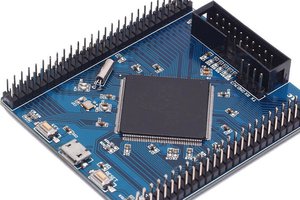
 Andy
Andy
 BaumInventions
 deʃhipu
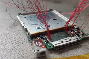
 Hugo Melder