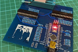
This project uses a Silego GreenPAK CMIC to split a WS2812B data stream into two feeds, one identical to the input and one delayed by a selectable number of LEDs. This allows one to string lights in short strings hanging off a bus, kind of like icicle Christmas lights.
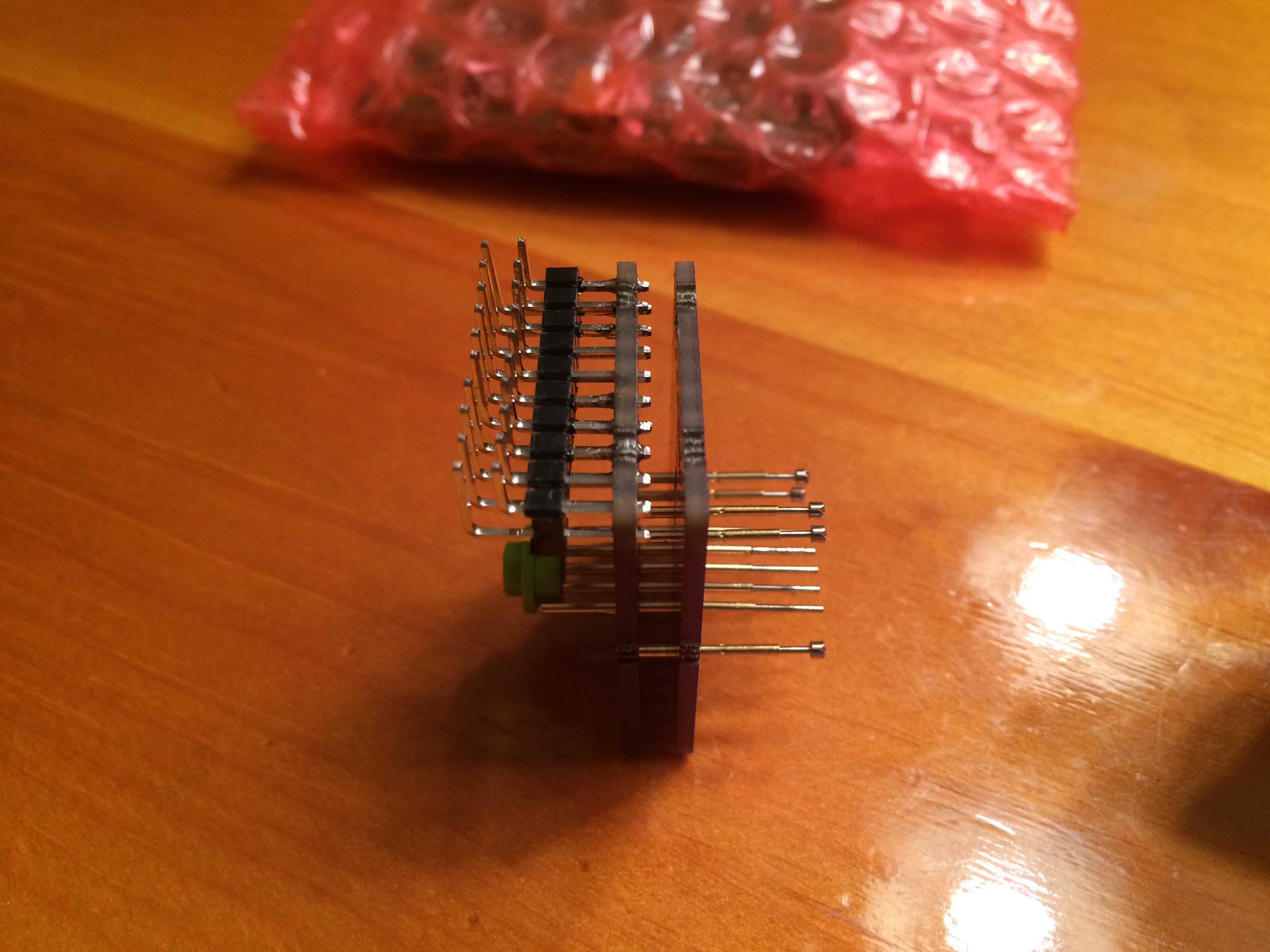
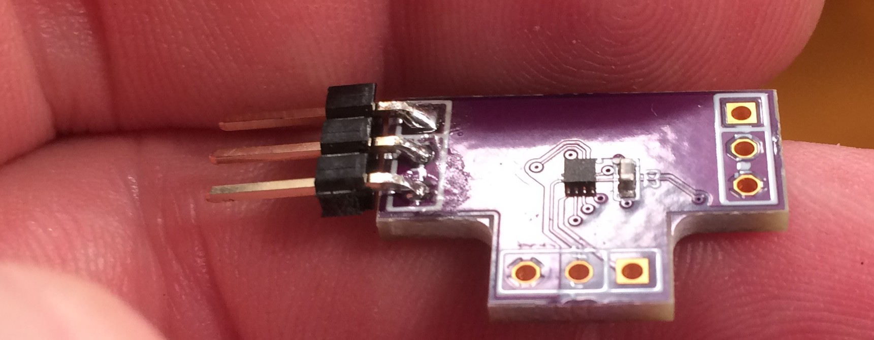
The Silego GreenPAK is a sort of FPGA that's got a very limited number of gates and can only be programmed once. The 12-pin SLG46120V used here is cheap, as you can get 5 for less than $1. I settled on that model because it had the largest number of DFFs, which I needed for the frequency dividers.
The GreenPAK Designer is a free download, and is used to layout the components, configure them, and connect them together, and create the bitstream used to program the chip. It also has the emulator portion that connects to the dev kit via USB for programming/debugging. The GreenPAK3 Dev Kit retails for $59 and includes 50 samples of each of four different chips.
The internals are covered in more detail in the project logs below. To summarize, the internal RC oscillator will trigger a reset when more than 10 microseconds have passed. The first pulse on D-In brings it out of reset until the next 10us blank. A counter creates a pulse every 24 input pulses, which is fed into a series of frequency dividers allowing a binary count up to 31 (2^5 - 1). The FD stages are compared to input pins (solder jumpers to ground) and raise another signal if all inputs match. When matching and the D-In pulse drops, a latch enables all following D-In pulses to also forward to D-Delay, until the next reset.


 Emilio P.G. Ficara
 John Lonergan
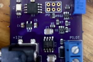
 Nick Sayer
Each pixel copies what it receives on DataIn onto DataOut, but only after it strips off the first 24 pulses (8 each for R, G, and B) for its own LEDs. The intent was to have this device strip off a predetermined multiple of 24 pulses on the delay out, similar to having that many pixels inline. Unfortunately, I never got it working. I didn't have a working oscilloscope at the time, and have been too busy since to come back to this project, but still believe it has the capability of being the lowest cost solution for doing this.
@will if you just want to duplicate pixels, eg. have a curtain where the top pixel on all lines is the same, then all you need is a few buffers. This is intended to delay the output so for example the Out line starts at the first pixel but the delay line starts at pixel 32.
Renard Plus used to sell a Pixel Splitter board with three outputs. The original idea came from this post: https://diychristmas.org/vb5/node/10559. I've looked at STM hardware as well, as their advanced timer peripheral has four CCR outputs. It should work, but I just don't have time to fully develop it.