 Eric Hertz
UPDATE V: Here's a demo using a TTL input as an example of my original "weird circuit" in use
Note that by varying the input-voltage to greater than about 3.65V, the circuit's very similar to mine, current flows from the base through the collector. And at nearly 5V, current flows into the NPN's emitter.
UPDATE IV: I FOUND A USE for the weird PNP mistake!
--------------
UPDATE III: Found a REALLY HANDY REAL-TIME-ish SIMULATOR
and more simulation-links at the bottom.
UPDATE II: New Interesting circuit, at the bottom.
UPDATE: ROTFL, it's just diodes... more at the bottom.
---------
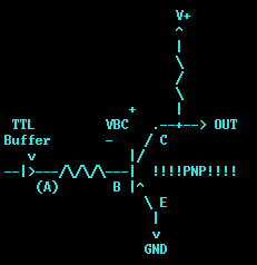
Over at #Improbable Secret Project, (Log: https://hackaday.io/project/18868/log/50780-open-collector-fail-the-atx-power-switch-saga-continues) I accidentally discovered that the following circuit is possible:
The key-factors are:
- Transistors work similarly when C and E are reversed (though with tremendously lower current-gain)
- TTL ... nah, that isn't really relevant, after all.
So, what we have, here, is a *buffer*, rather than an inverter, as it would be with the NPN I'd intended to use.
It's sort of an emitter-follower, except using the "key-factor" this makes it more of a "collector-follower."
(BUT, allegedly that term is reserved for another purpose.)
Note that when the input voltage is greater than (V+ - 0.6V) (high, assuming VBC-on=0.6V), the transistor is *off*.
When the input is less than (V+ - 0.6V) the transistor is *on*, and the output-voltage follows the input voltage... So, a 0V input would result in a 0.6V output (which is lower than a TTL circuit's VIL-max of 0.8V, nice) so it will be Low.
Similarly, a TTL circuit's VIH-min is something like 2.0V, and obviously VOH-min must be greater than that. So, feeding 2.0V into the input, the transistor will be on, but its output-voltage will be 2.6V... High.
(Of course, these depend a little bit on the value of the base-resistor)
----------------
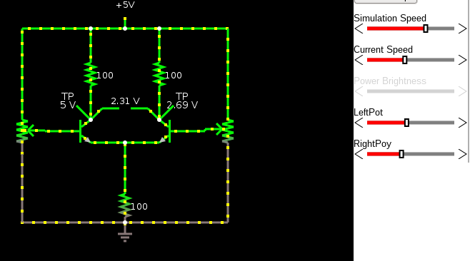
Well, here's an interesting result...

This is an AND gate, I think!
I'm calling it a [L]AND gate, because, without the pull-up resistor, it's an AND which only outputs the Low state, the "high" state is determined by the load (the pull-up resistor, in this case).
Similarly, if I've got my logic right, the opposite (using NPNs connected to V+), creates a [H]OR gate.
I'll stick to discussing the [L]AND gate...
When both inputs are the same, we have the same effect as with a single transistor... That takes care of the 00, and 11 states of an AND gate.
My THEORY (untested) is that the lower of the two inputs will be followed.
The reality may be significantly different... Since the current-gain is really low (like IC=2*IB), and since the high input would imply a higher current going into that transistor's base, that transistor (the one pulled high) will have a greater IC... and this is where I can't quite wrap my head around it... because a higher IC (through B) would create a greater current through C->E, which would cause it to pull even lower. Hmmm...
So, I think it's an AND gate, but I'm not certain.
------------
This came as a result of analyzing @Ted Yapo's circuit from #CBJT Logic:
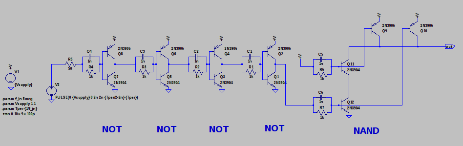
Note the normally-biased PNPs Q9 and Q10 in that circuit form a NAND gate. Which seems a bit backwards, since they're in parallel. But if the other transistors were removed and replaced with a pull-down resistor (and if this were 5V logic), then we'd have essentially the exact opposite of the [L]AND gate... they'd be a [H]NAND gate.
Now, I find it a bit strange that two *parallel* transistors could create an AND (or NAND) gate... OR, sure. NOR, sure... So I took a bit to think about it and, here's my conclusion. NAND is actually the same as an OR which has its inputs inverted.
      ______
-|>o--\     \
      | OR   >---
-|>o--/_____/

    =
      ______
-----|      \
     | NAND  |o--
-----|______/
Unfortunately, it doesn't seem [to me] too simple to interface a [L]AND and [H]NAND gate such that the series transistors (and pull-resistors) could be removed... but I could be mistaken. Maybe somehow within Ted's 1V logic...?
But, there enters a new problem for the [L]AND gate... its output is Low=0.6V minimum, but if I understand correctly, in CBJT logic, that'd actually be a *high*. And, further, the [L]AND's output is highly dependent on the load... its being pulled-up via resistor means the resistor supplies the current to the next stage when the output is low, not the transistor... which means despite its output being low, the current is flowing *out* of the "output". which means it can't pull another transistor's base low, right? And might not even work with TTL inputs (which are NPN emitters)... And, again, here's where my head starts spinning.
---------------
Update: I dunno how I didn't see it before... basically my circuits are nothing more than diodes...

----------------
Here's an interesting one for yah, from @Yann Guidon / YGDES
What's this do? (Answer in the comments! Scroll-carefully if you don't want the spoiler!)

(Hmmm, might not need the resistors on the inputs)
--------------
Here's a simulation of one of @Ted Yapo's #CBJT Logic inverters.
And here's a simulation of his NAND circuit
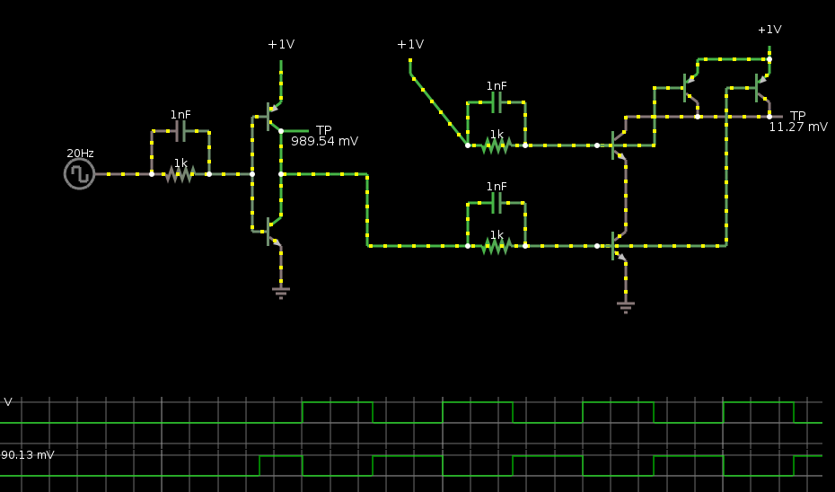
These screenshots don't do it justice... The little dots in the wires move to show the current-flow, which is quite handy in viewing this circuit's functionality.
I'm not sure I'd use this to do simulations of nitty-gritty details, but for demonstrating fundamental concepts it works really well.
------------
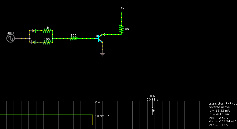
Here's the "fundamental concept" that I couldn't wrap my head around, with the PNP and its emitter tied to ground. Actually, this demo shows what's happening, and it isn't "just a diode" after-all! Too bad it doesn't export animated GIFs... so click that link, if you're curious.
Discussions
Become a Hackaday.io Member
Create an account to leave a comment. Already have an account? Log In.
Yep, if the resistor is on the high side, the current is shared by the inputs and limited inherently :-)
Are you sure? yes | no
brilliant!
Are you sure? yes | no
it's something I recognize now, after playing with ECL circuits and differential pairs :-D
Are you sure? yes | no
so In1 and In2 can be E and C of the same transistor ...
Are you sure? yes | no
the last image? Interesting... so the output of the circuit is the base?
Are you sure? yes | no
yup
that's why I bought my first germanium transistors : to get a pair of germanium diodes and confuse the hell out of people :-P
Are you sure? yes | no
haha, funny! And definitely confusing. Does germanium allow for larger base-currents?
Are you sure? yes | no
no and they leak like hell (particularly the early ones, not to mention the russian ones) but they contain 2 diodes, look very odd (russians...) and are super-vintage-looking :-P
Are you sure? yes | no
Gonna have to take a closer look at your germanium projects and see how often you use that trick ;)
Unrelatedly: Checking out some pictures over at #Germanium ECL, I see ECL uses NPN emitter-followers tied to V+ as outputs. interesting... They shoulda swapped their emitters and collectors ;)
Are you sure? yes | no
i don't use it yet, i considered the naughty trick only for a general RESET of the many FF : one transistor instead of 2 diodes...
swap : why ? the way it is, a very high gain is provided, shielding the differential pair from the output parasites.
Are you sure? yes | no
Because it would've satisfied my search for a danged use for my danged circuit ;p
Are you sure? yes | no