 slisgrinder
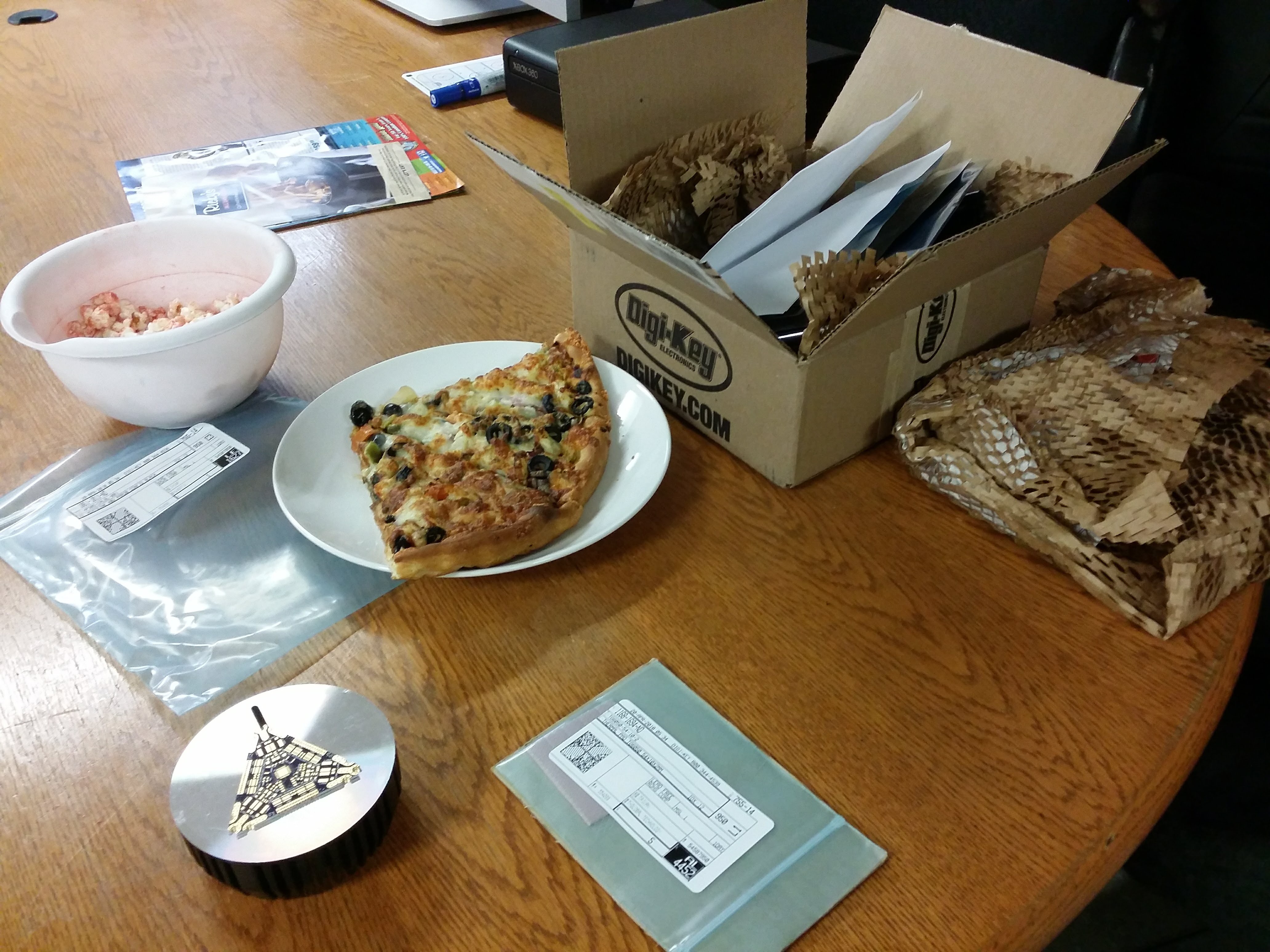
This project initially stemmed from my unconditional love of Okra before it became what is now MOSAIC LS. I wanted to see if I could grow Okra in the cold, dry climate of Alberta, Canada but It proved to be more difficult than originally thought.
Before we dive into the 'deets, lets start off with some common nomenclature which will be used throughout. The assemblies are arranged in the same manner as photo-voltaic applications:
- "Cell" - PCB containing the emitters and uC
- "Module" - collection of interconnected cells in the shape required by application
- "Panel" - collection of interconnected modules
- "System" - collection of interconnected panels
Due to safety, legal and long term reliability concerns, the UV emitters were removed from the grow light variants and a 4th variant was added (GUVL - General Purpose UV Light). This new UV variant includes design elements that will protect against UV degradation as well as additional safety interlocks. This should make using the GUVL variant safer with increased reliability.
The 4 proposed variants are:
- AHLS - Adjustable Hue Lighting System:
- ~625nm red emitter
- ~525nm green emitter
- ~470nm blue emitter
- 5000K - 5700K white emitter
- GTGL - General Purpose Terrestrial Grow Light
- ~740nm far red emitter
- ~660nm red emitter
- ~525 green emitter
- ~470nm blue emitter
- ~450nm royal blue emitter
- ~5000K - 5700K white emitter
- GAGL - General Purpose Aquatic Grow Light
- ~660nm red emitter
- ~525nm green emitter
- ~470nm blue emitter
- ~450nm royal blue emitter
- ~425nm violet emitter
- ~5700K while emitter
- GUVL - General Purpose UV Light
- ~385nm UVA emitter
- ~310nm UVB emitter
- ~280nm UVC emitter
For this project, we will be looking at the GTGL variant as it encompasses all aspects of design that are common to the other variants.
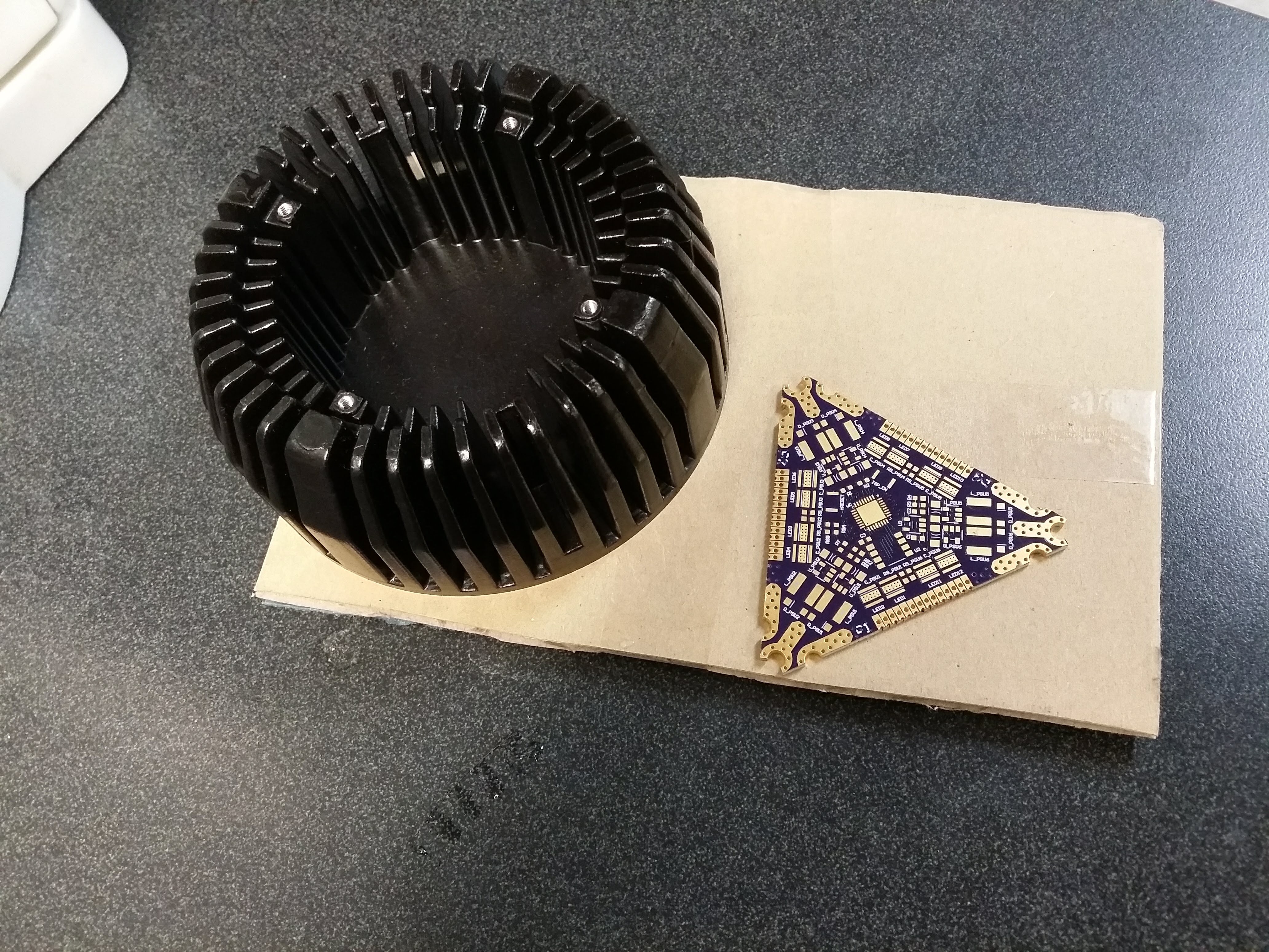
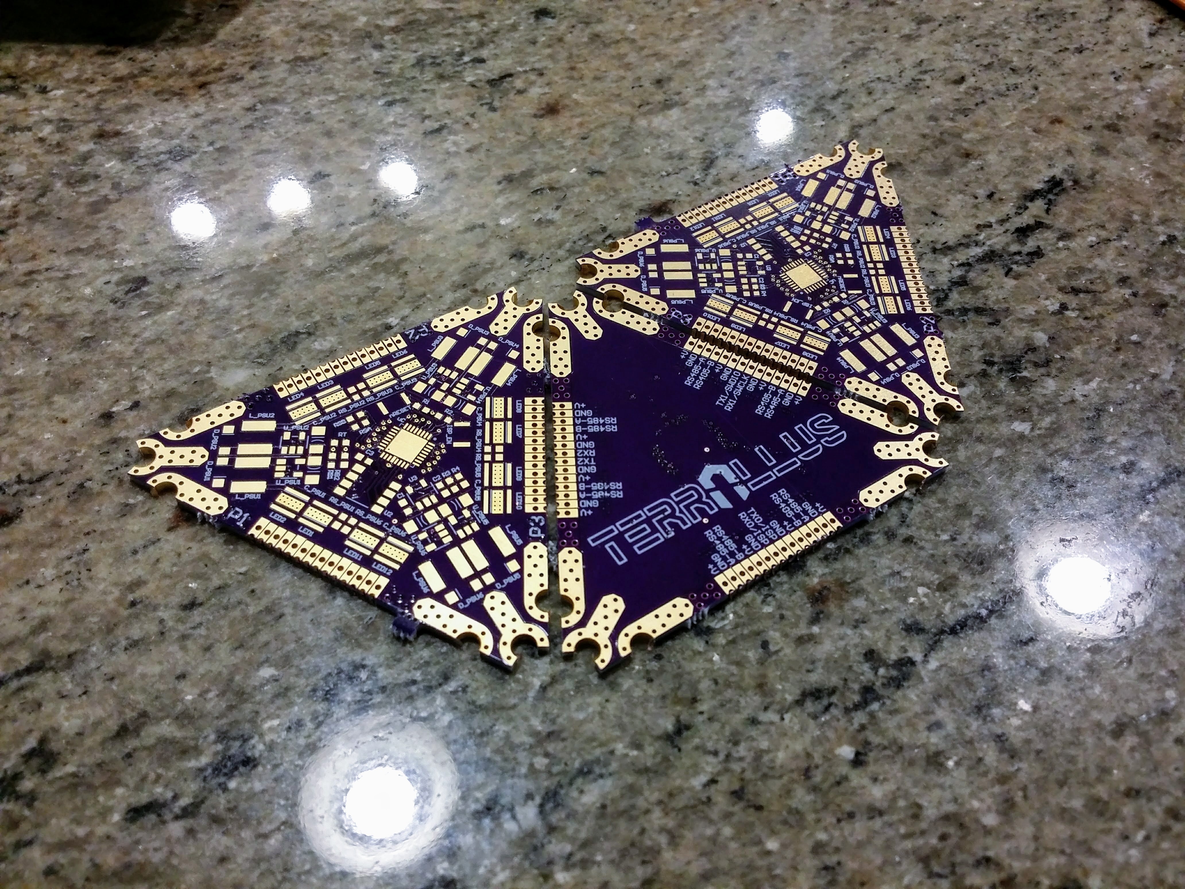
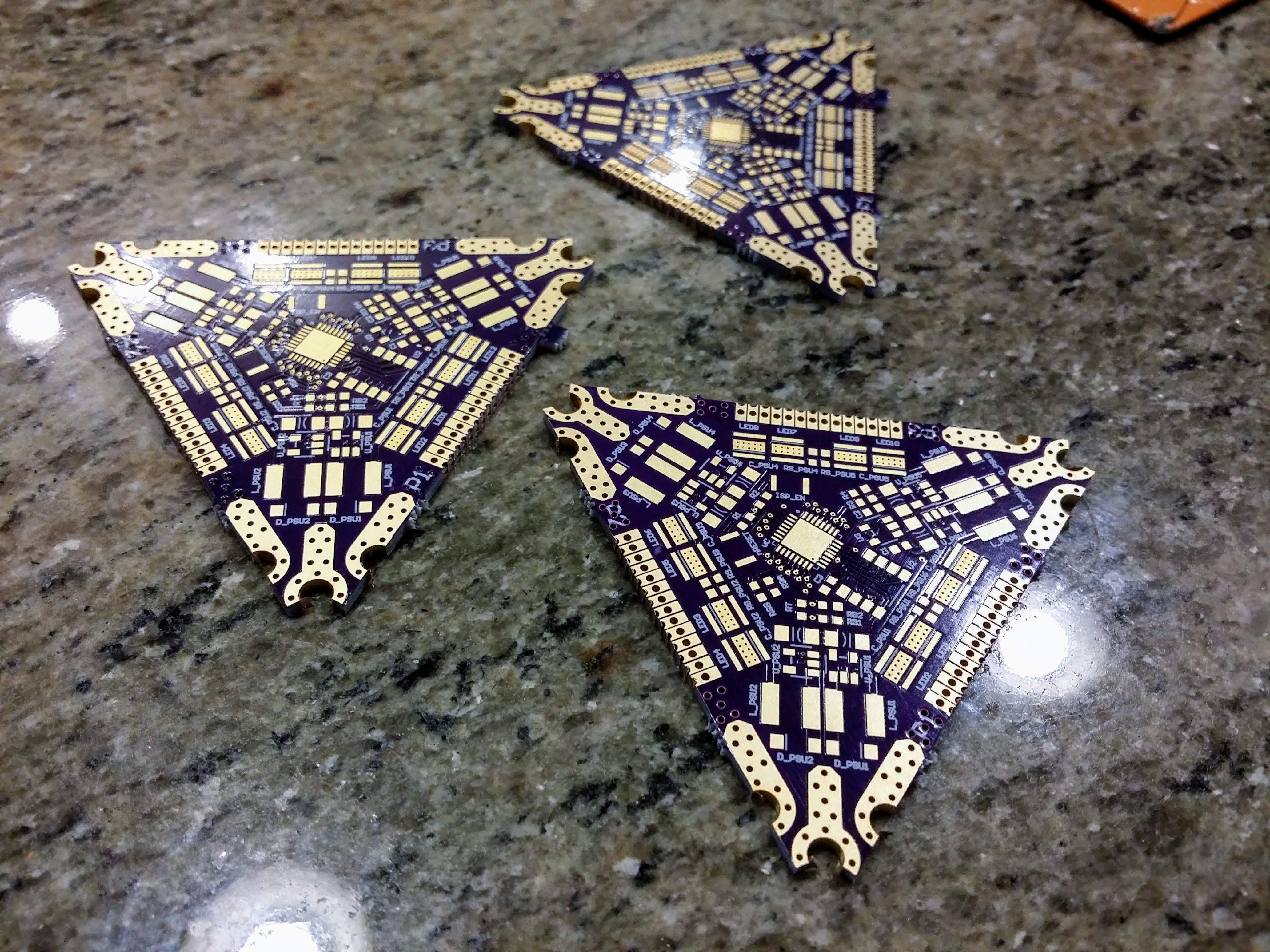
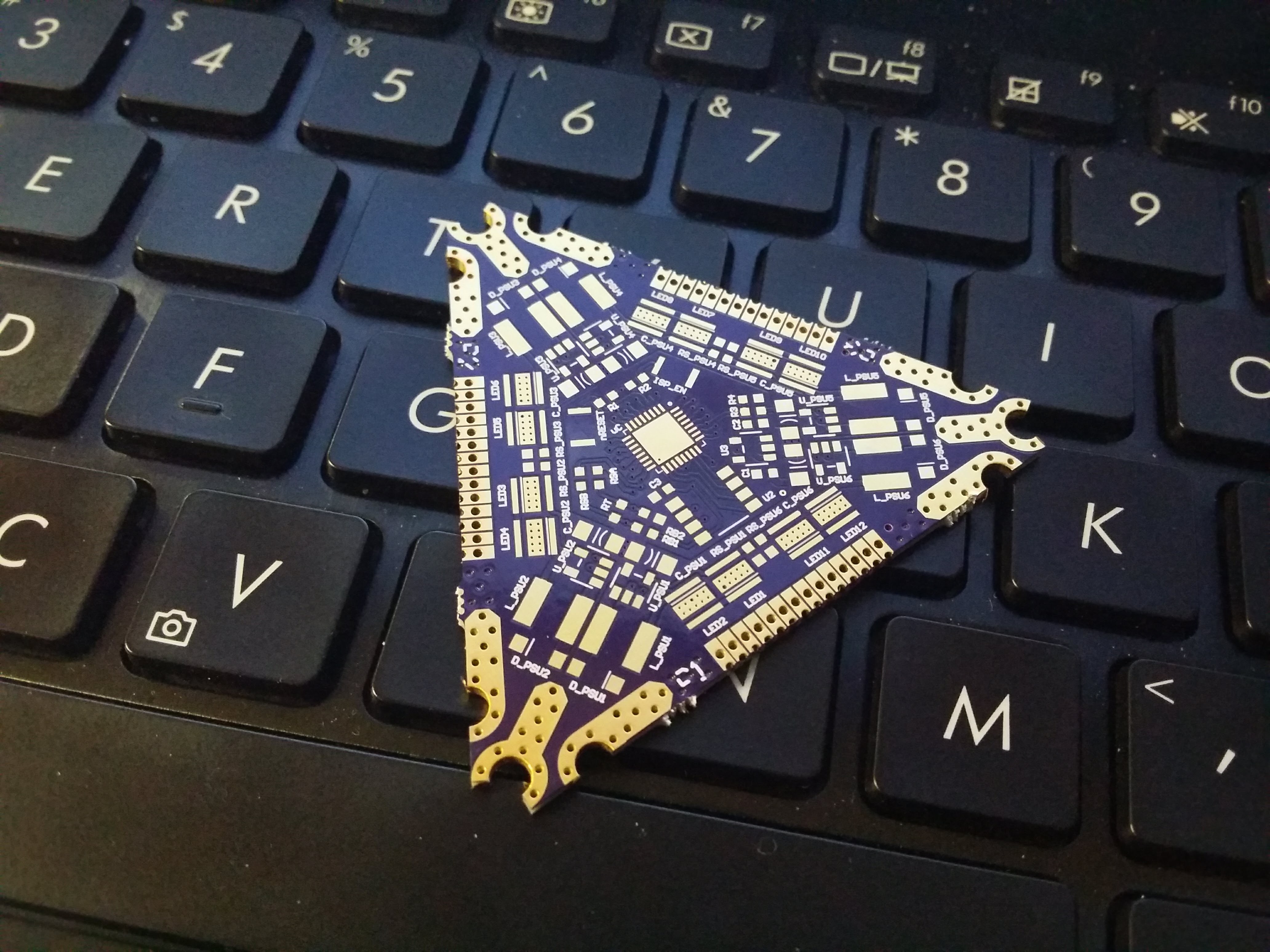
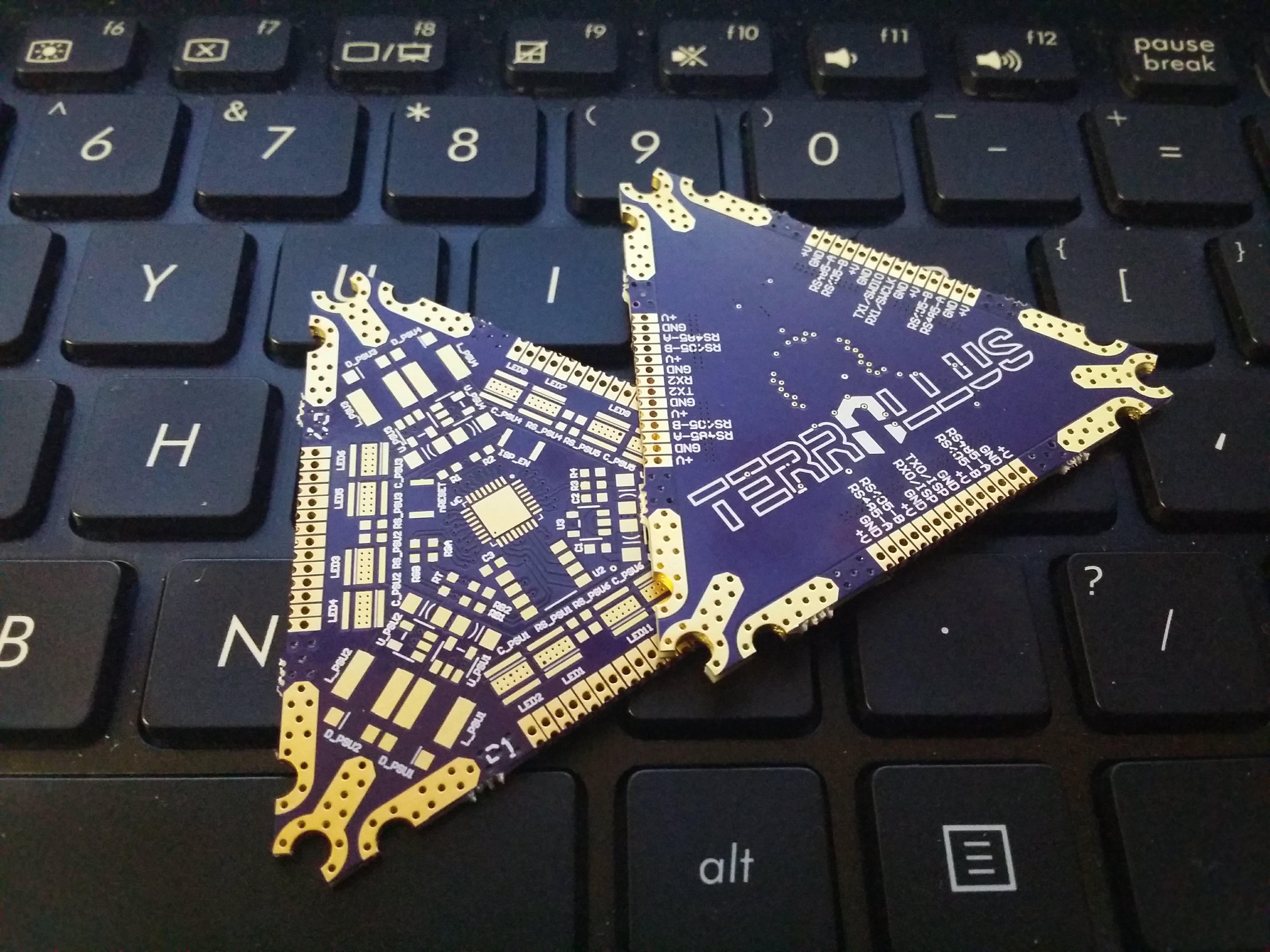
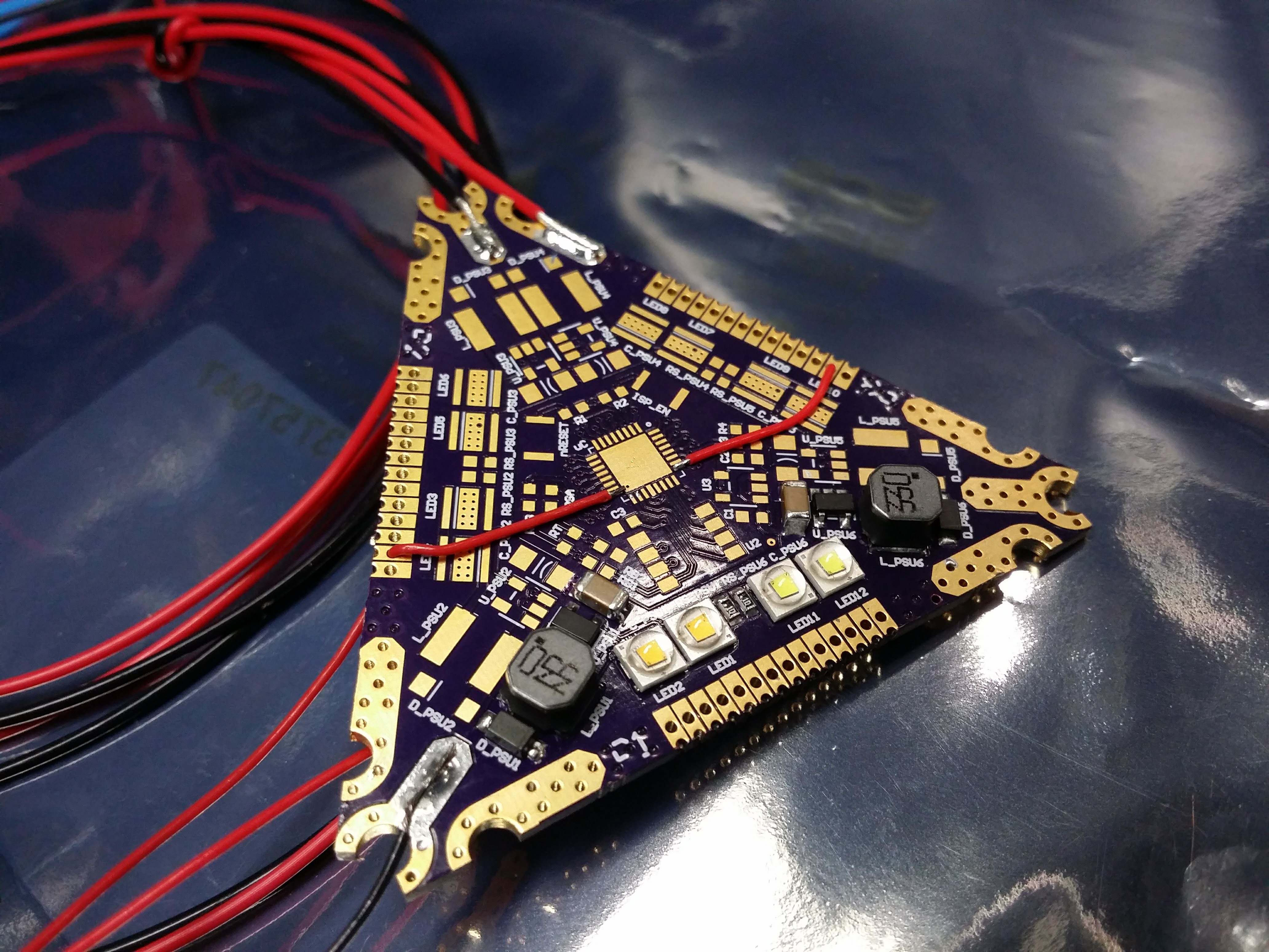
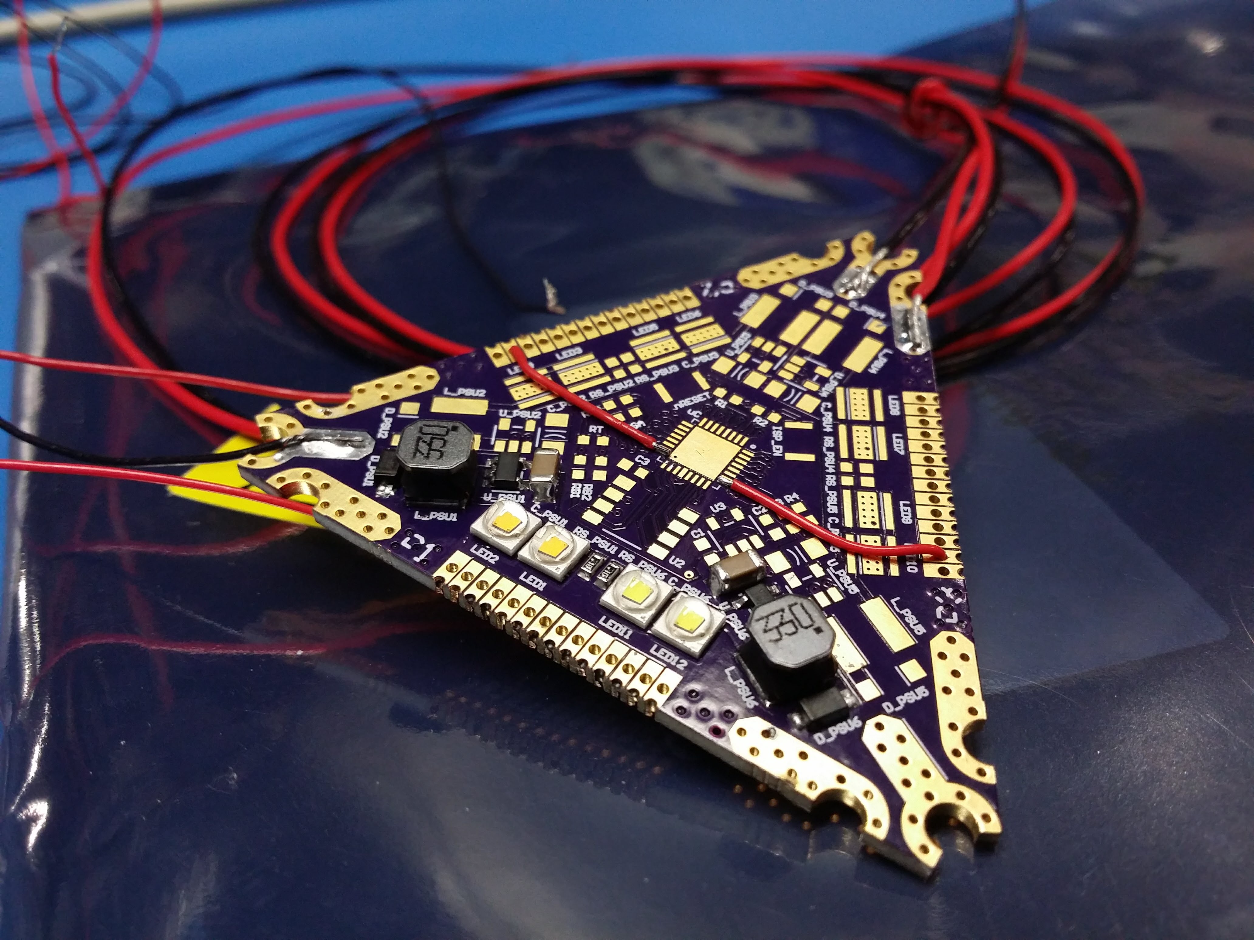
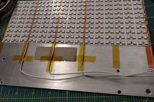
The cell is composed of a triangular PCB which contains:
- a uC (microcontroller)
- various emitters as per product groups
- 3x connectors
- one connector on each side
- each connector with symmetric pin layout to enable connection to other cells without worry of orientation

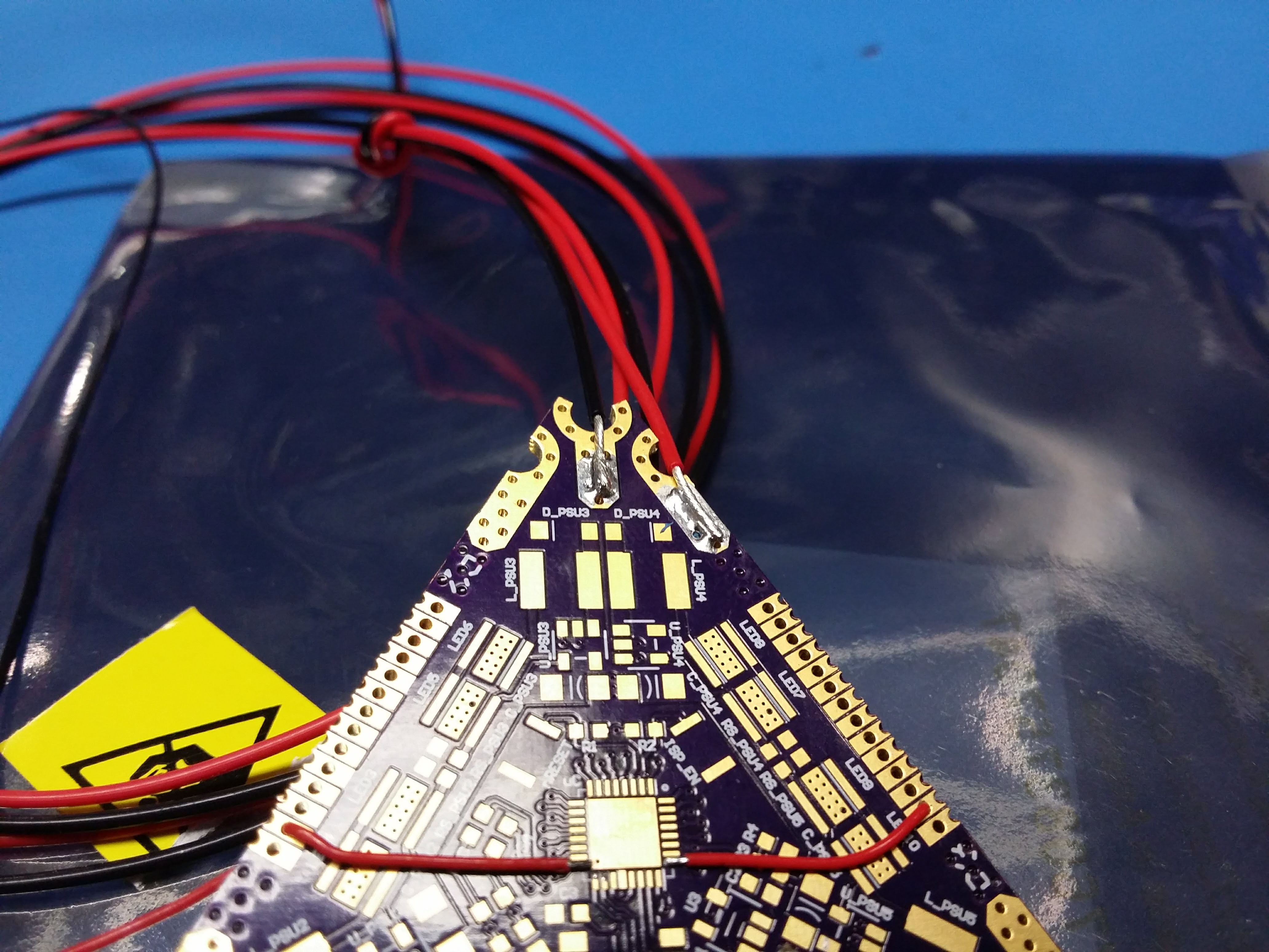
It's physical dimensions are based on an equilateral triangle (Figure 1, outlined in gray) whose sides measure 62.5 mm. The corners of the triangle are equipped with holes to accommodate an M3 socket head cap screw. This screw is connected to ground ("GND") of the cell. Adjacent to the ground screw are identically sized holes but half-way to the edge and connected to main power ("+V") which in this case is 12V DC nominal. This simplifies carrier/housing design and power supply routing. Wires can be soldered on either side of the PCB or a carrier board with spring clips can be designed where the cell just clicks into place.

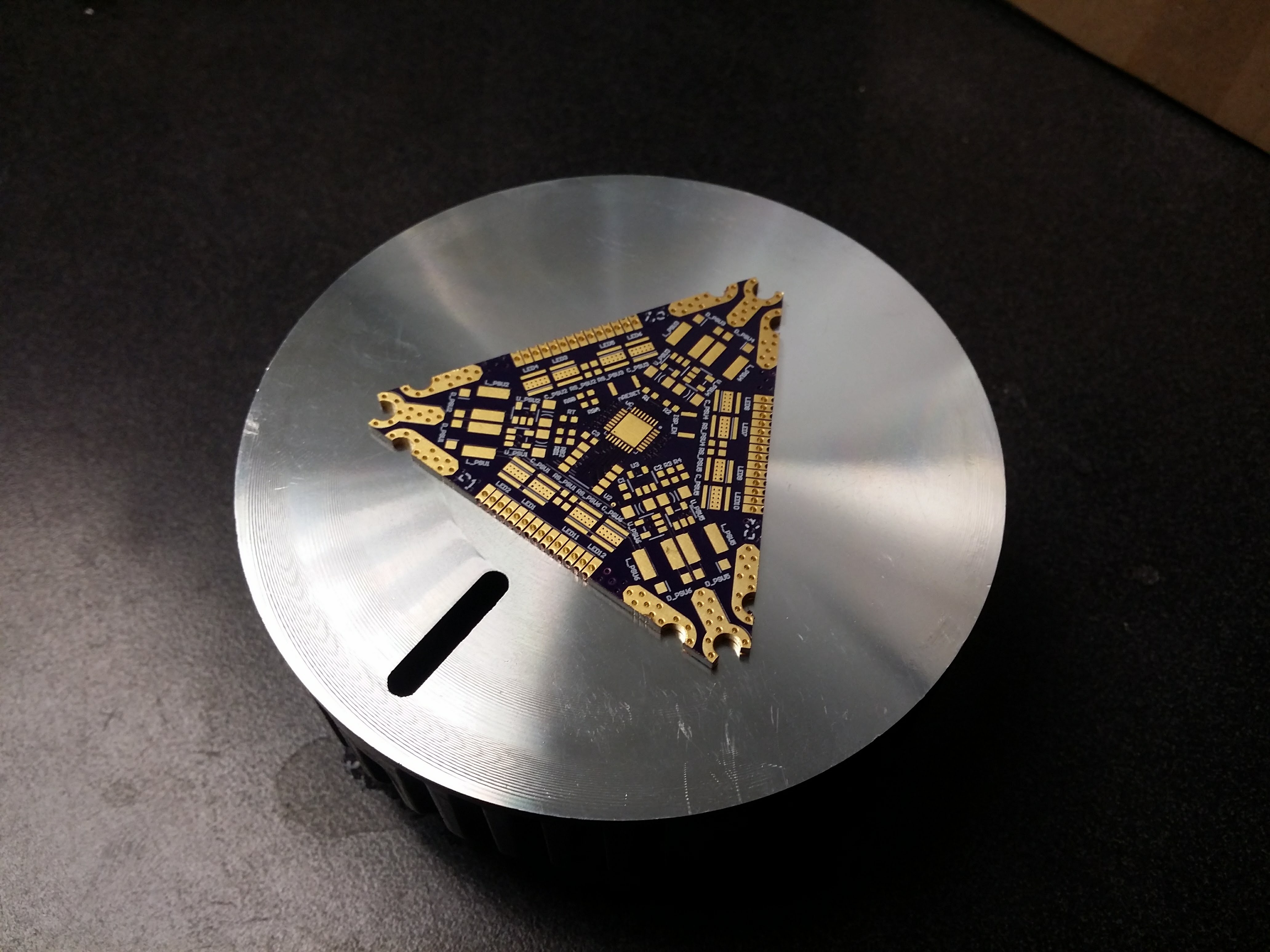
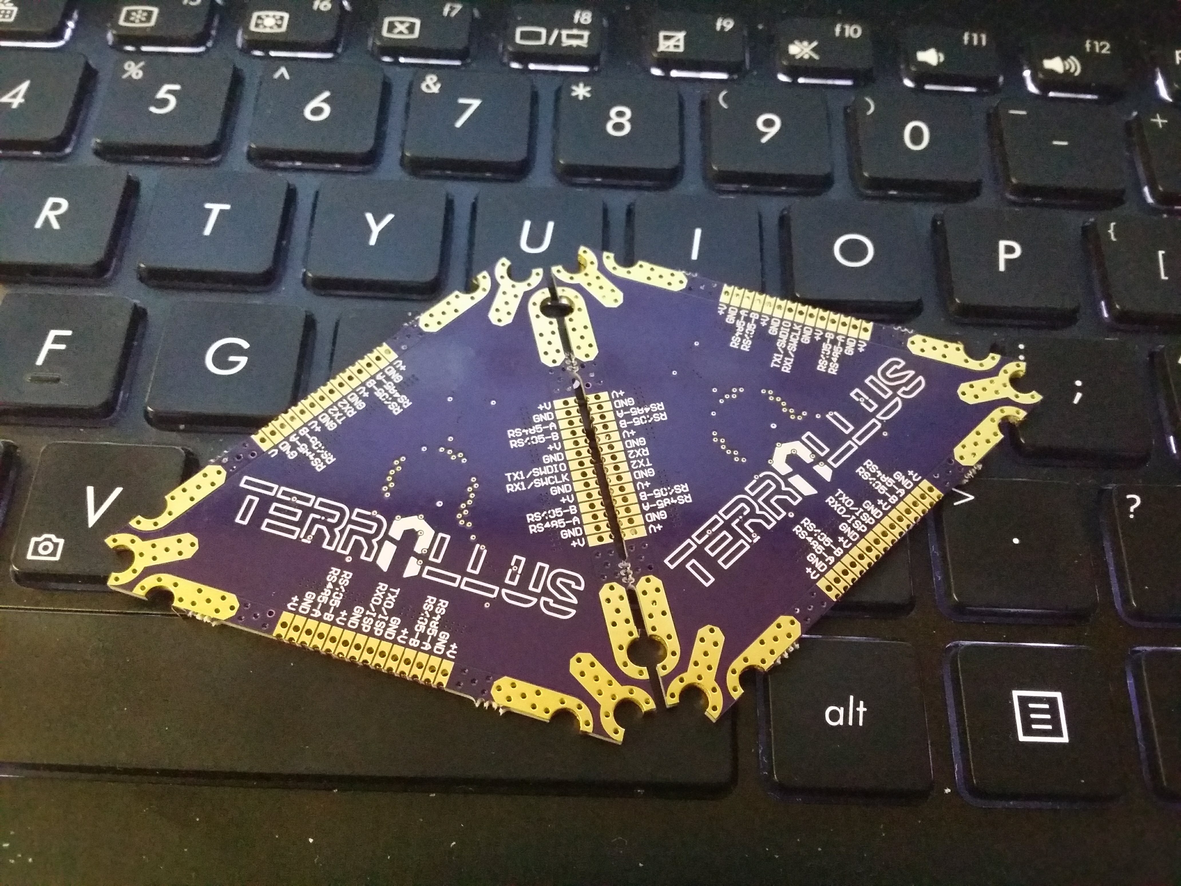
The connector design and layout are chosen to allow maximum application flexibility. It is a hybrid through hole/surface mount pad with symmetrical pinout. Designed to allow 50mil pitch headers to be soldered directly to the cell via the available through hole/SMT pads. In addition, flat cables with similar pitch can also be soldered directly. See Figure 2 above for pad pitch screen cap.

The connector pinout (Figure 3) is laid out to allow adjacent cells to be "butted" up and directly soldered without the limitation of orientation of the cells. See Figure 4 below for an example of "butted" connection.

Cells communicate over RS485 using MODBUS as the protocol of choice. This allows for communication with each cell regardless of how deeply embedded they are in their application and can be dropped into existing MODBUS networks. For local communication (single cell interface, cell to cell etc.), the RS485 line driver can be bypassed and 3.3V UART used...
Read more »


 Quinn
Quinn
 Stephen Harrison
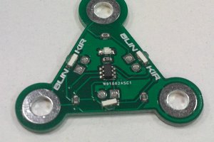
 Gee Bartlett
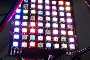
 Chris Hamilton
Thank you everyone for the follows and likes. It really means a lot to me and is very motivating to continue development on this project.
Cheers!