 Nick Sayer
The Backpack variant
The J1772 pilot line on the EVSE end is connected to a ±12 volt square wave generator with a 1 kΩ output impedance. The line can either be pinned at +12 volts, -12 volts, or oscillating at 1 kHz with a variable duty cycle. If no vehicle is connected, or if the EVSE is not ready for charging, it will pin the pilot at +12. If the EVSE is in an error condition from which it cannot reasonably recover, it may pin the pilot at -12 volts. If a vehicle is connected and the EVSE is prepared to supply power, it will oscillate the pilot.
On the vehicle end the circuit is quite simple. There is a 2.7 kΩ resistor in series with a diode from the pilot to ground. Most EVs will have a second 1.3 kΩ resistor in parallel with the 2.7 kΩ one, but with a switch (likely a transistor or MOSFET) to bring the 1.3 kΩ additional impedance into play. Because of the host EVSE's 1 kΩ output impedance, 2.7 kΩ will lower the +12 volts to +9 volts. The added 1.3 kΩ will reduce that to +6 volts. Optionally, a fourth state can be defined by adding another 330 Ω, reducing the voltage to +3 volts. This last state indicates to the host EVSE that this vehicle has lead-acid batteries and requires ventilation for charging. EVSEs mounted indoors are supposed to refuse charging when this happens, but EVSEs mounted outdoors can allow it.
The diode will prevent the added impedance from impinging on the negative portion of the square wave. The EVSE is able to detect the minimum and maximum voltage seen on the vehicle side of the 1 kΩ output impedance and therefore detect the state changes. If the negative portion doesn't reach (close to) -12 volts, then the EVSE can surmise that the diode is missing and that a compliant vehicle is not connected and refuse to charge.
The duty cycle of the 1 kHz square wave indicates the ampacity of the EVSE from 6 amps to 80 amps. Additionally, a special duty cycle can be used to indicate "digital communications required," which is what CCS HVDC EVSEs use.
The EV Sim uses a resistor divider network to rescale the potential input voltage range of -12 to +12 to 0-5 volts. Because the impedance on the input side is 200 kΩ, we must provide an impedance buffer amp (that is an op amp configured for unity gain) in front of the analog input pin on the controller. Not doing that results in the previous voltage of the ADC sample-and-hold cap dragging the scaled voltage away for a few microseconds while the cap charges/discharges to the new level. This is brief, but it's still potentially enough to trigger the analog comparator, which results in weird duty cycle aberrations. The controller is also fed a comparison voltage that represents (near) 0 volts on the pilot line. The controller's analog comparator will output a low or high logic level based on this comparison, which essentially means that the pilot is above or below 0 volts. This comparison is used to trigger an interrupt in the firmware and to capture the value of a free-running timer. The number of times this interrupt occurs during a given sampling period is double the frequency over that period, and the difference between the capture and the previous capture allows the ISR to keep a running timing that represents the duty cycle of the wave. During the sampling period, the controller samples the input voltage repeatedly and captures the maximum and minimum voltage. The EV Sim is a "backpack" board on a 2x16 80x36 mm LCD character display. It will display the frequency and duty cycle of the pilot (if it's oscillating) and translate that into a J1772 ampacity indication. Pressing the button will change it into a mode where it displays the minimum and maximum voltage.
The Remote Variant
There's a second version of the project that exchanges the LCD for a USB connection. The ATTiny84A is replaced with an ATTiny841, which has a USART in it to make serial I/O easier. The serial pins...
Read more »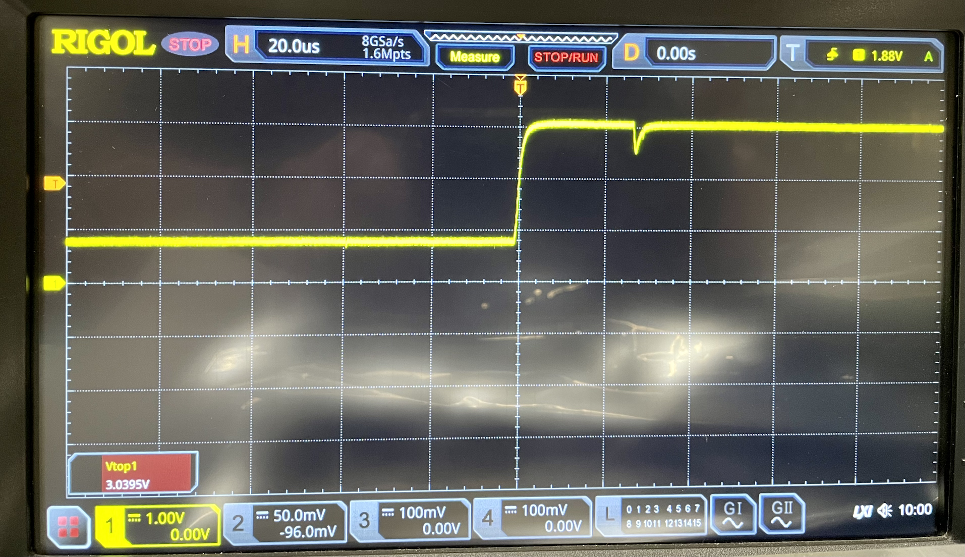


 Tijl Schepens
 Christoph Tack
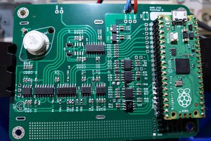
 NNNI
NNNI
Been playing with the idea of replacing swtiches too; ended up with this simulation. Hopefully build circuit soon and test in real life
http://preview.tinyurl.com/hpb7bkg