 Grant Giesbrecht
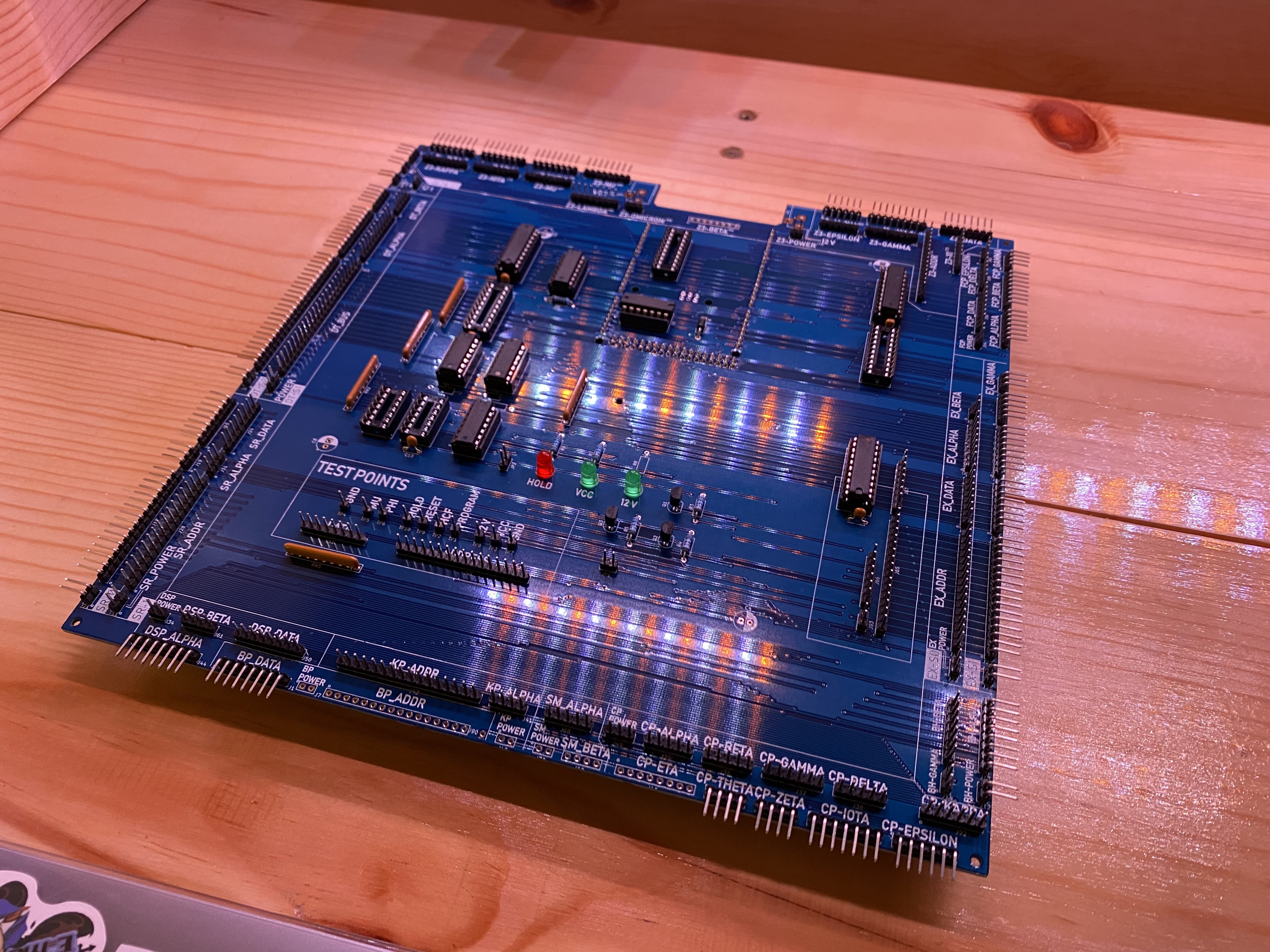
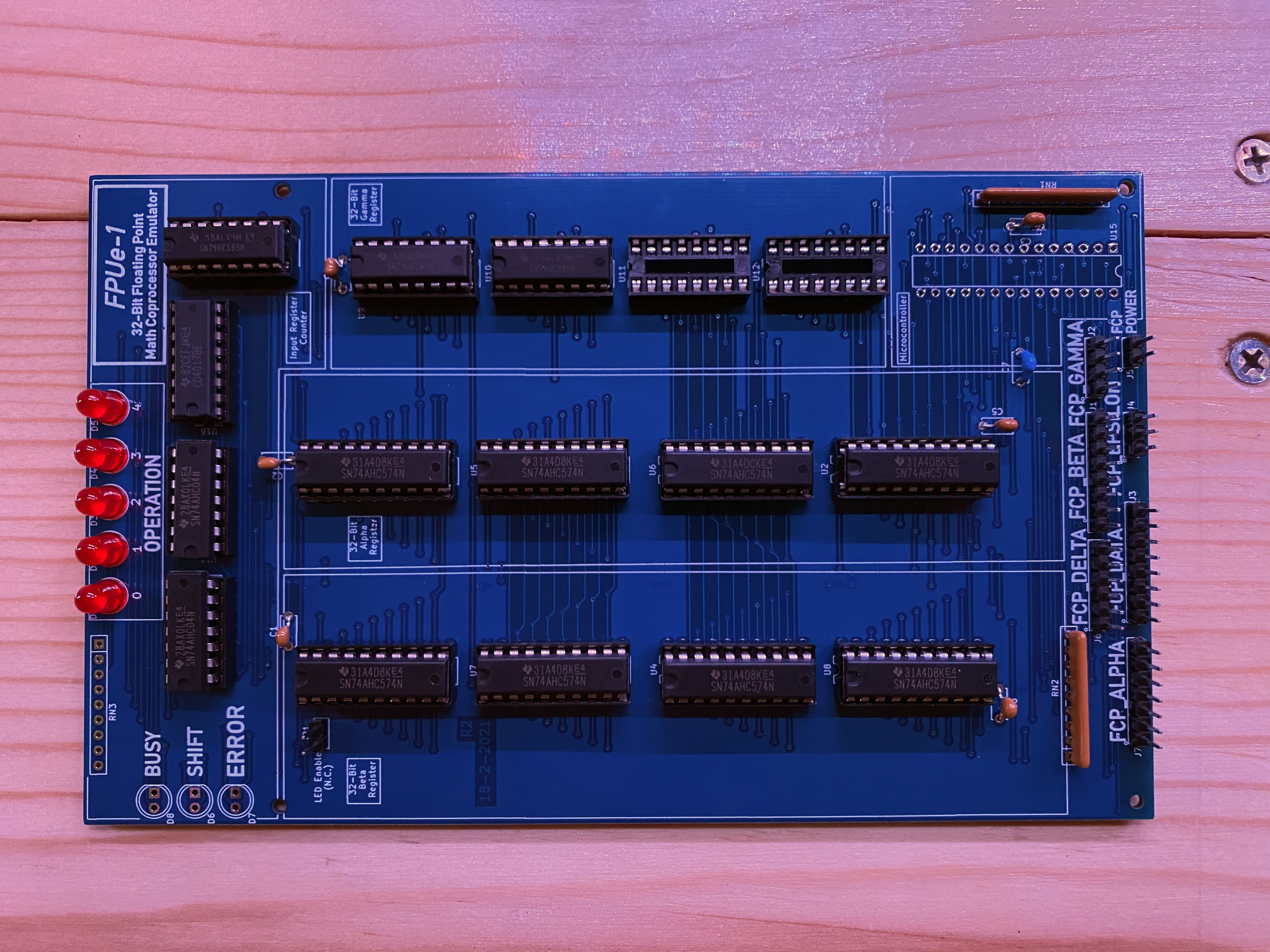
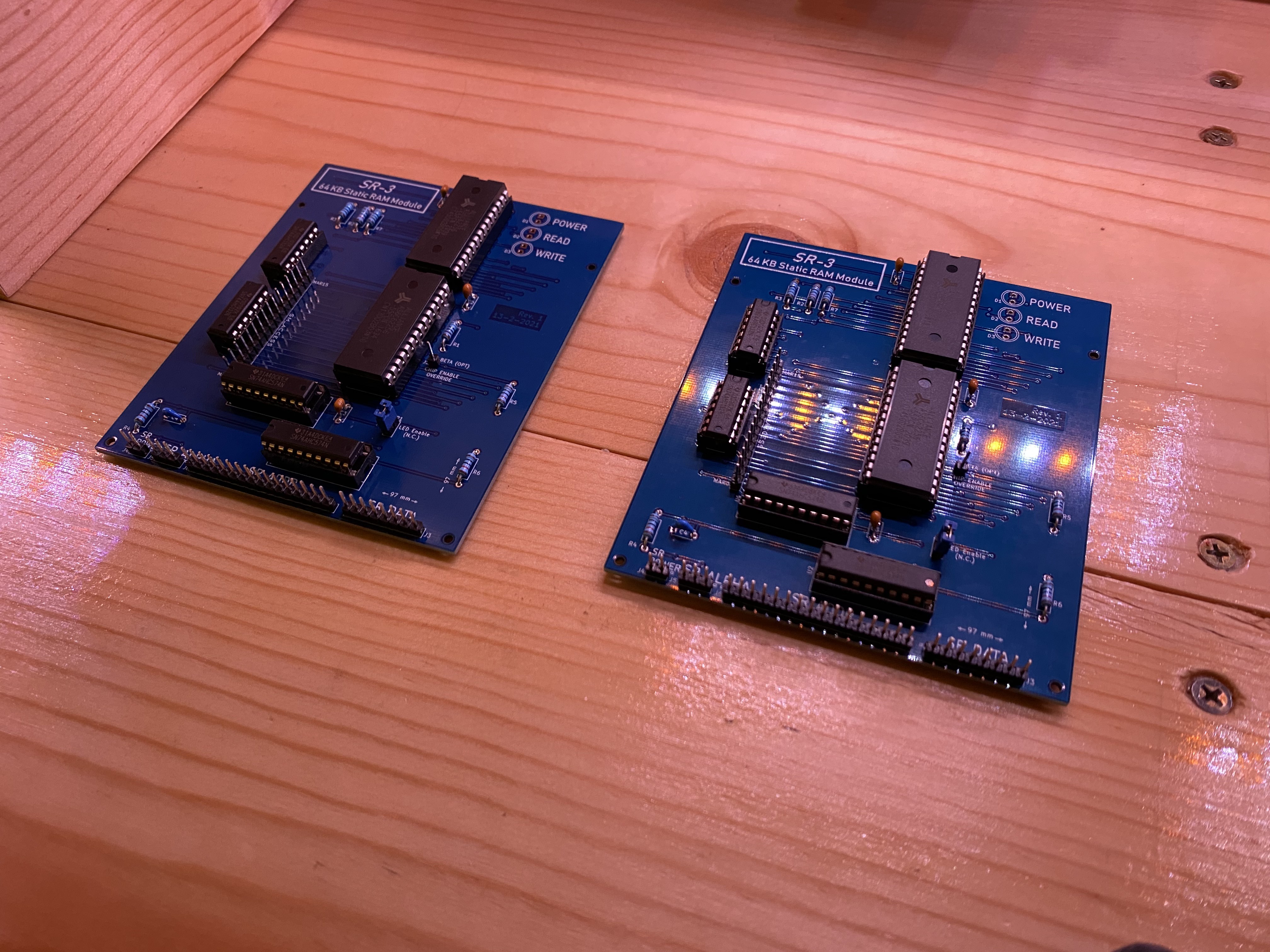
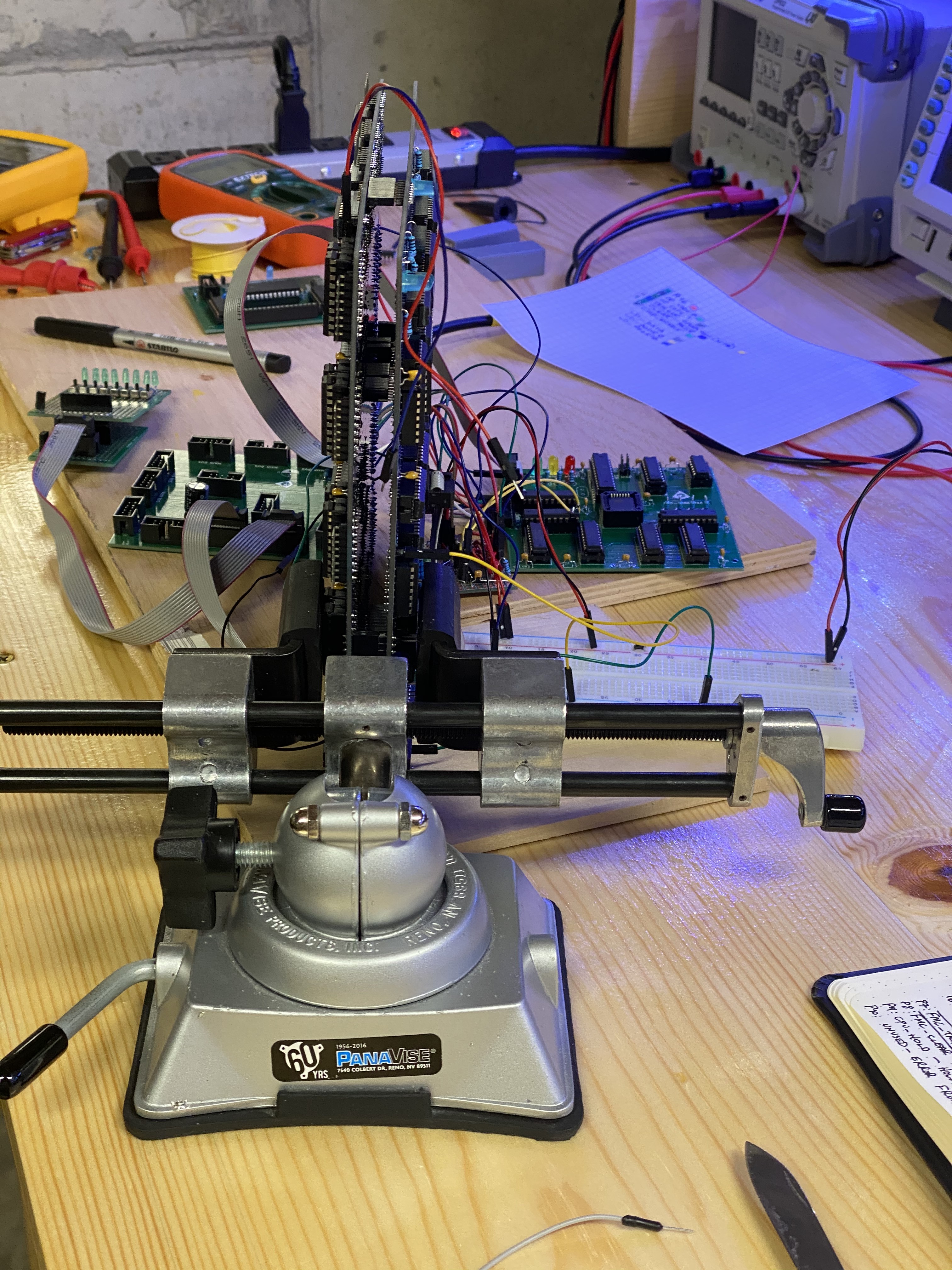
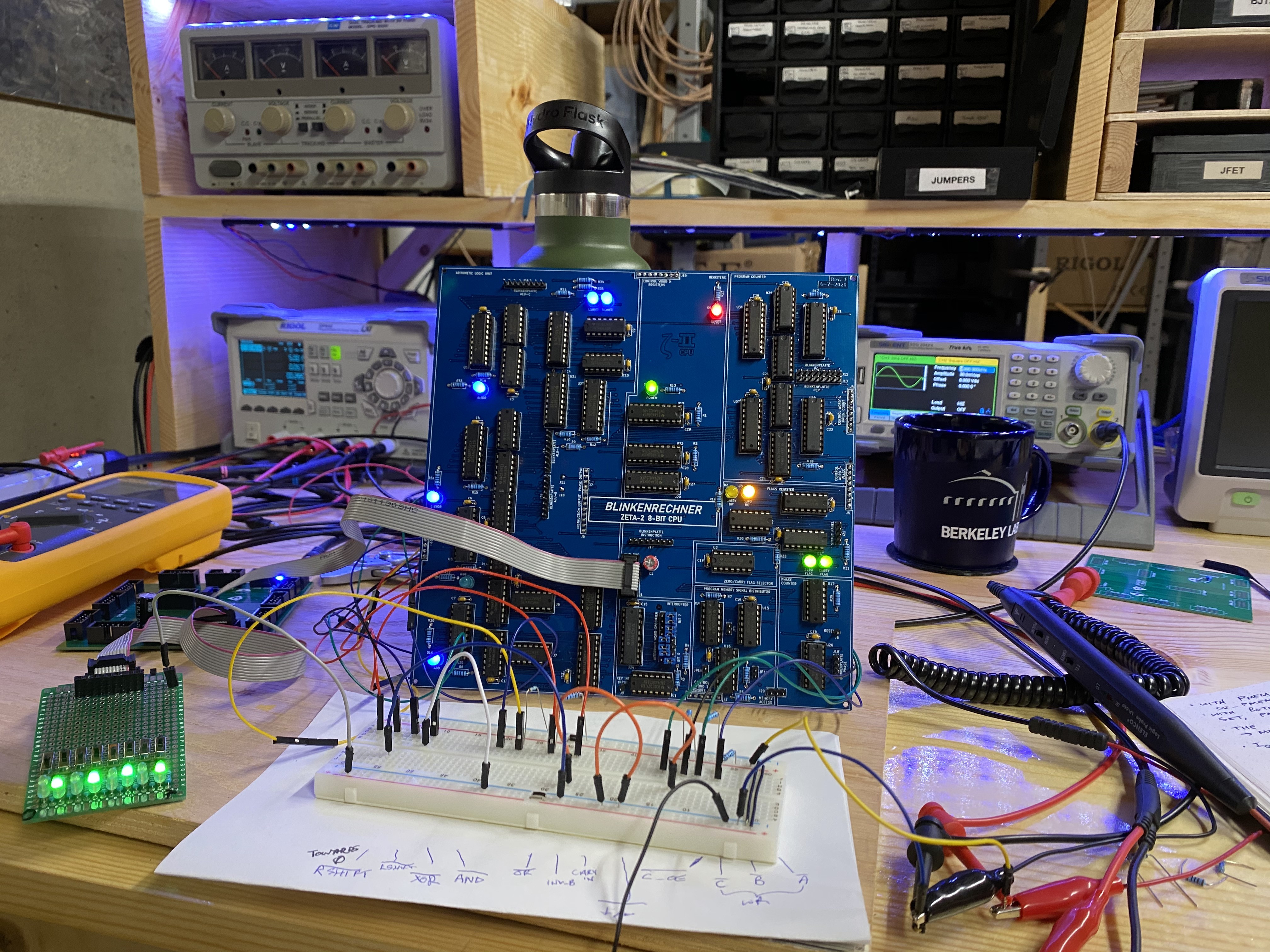
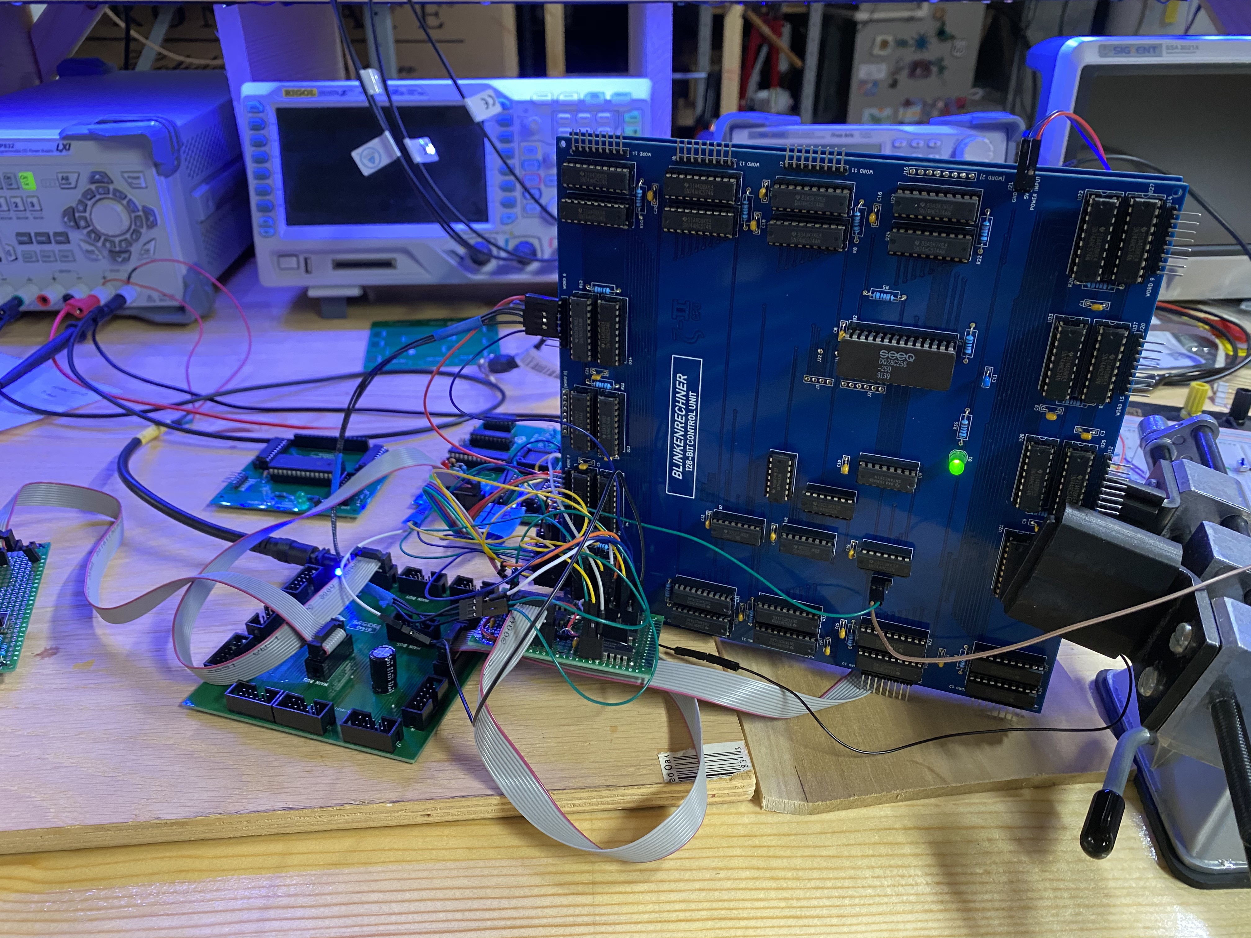
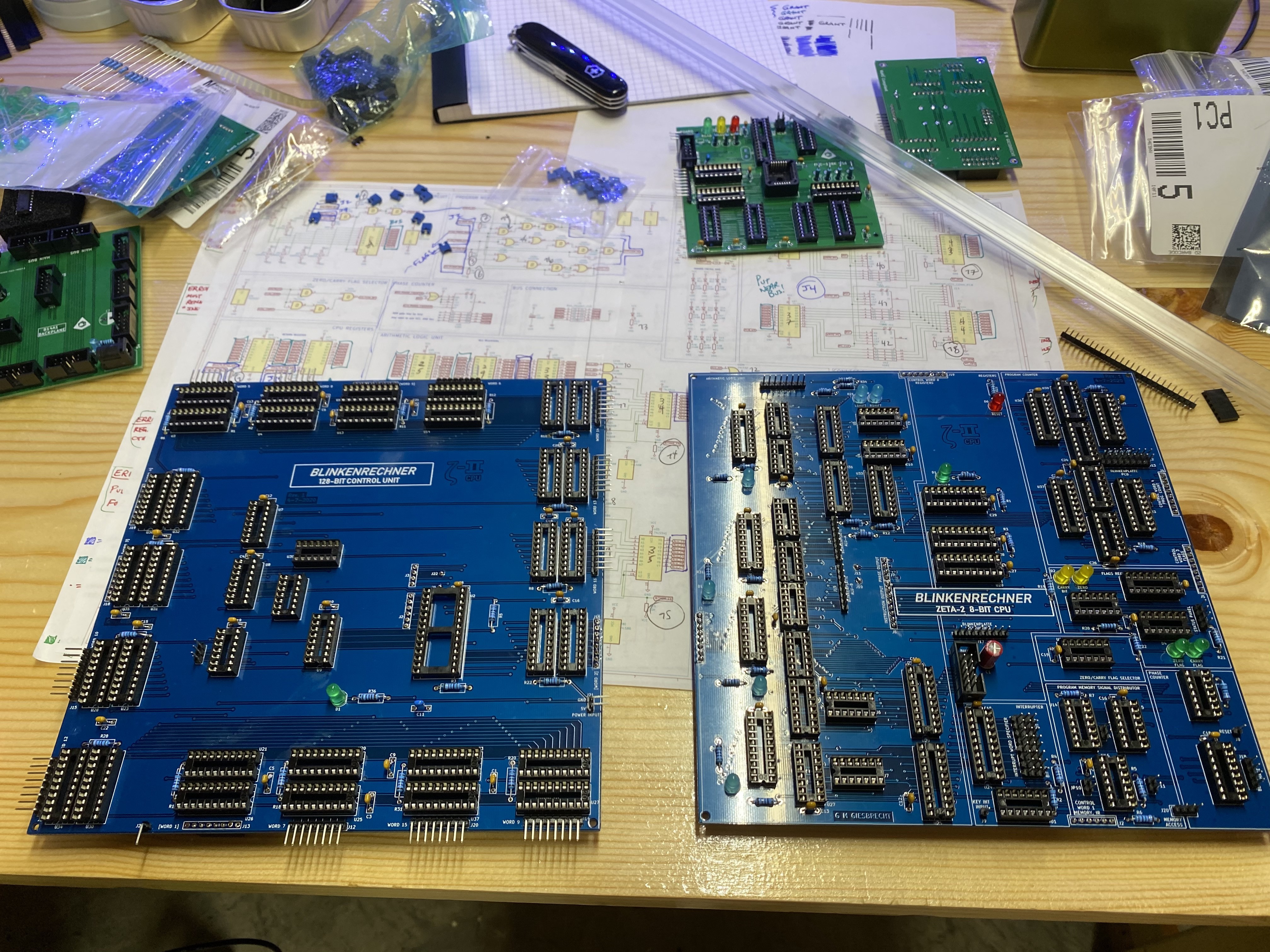
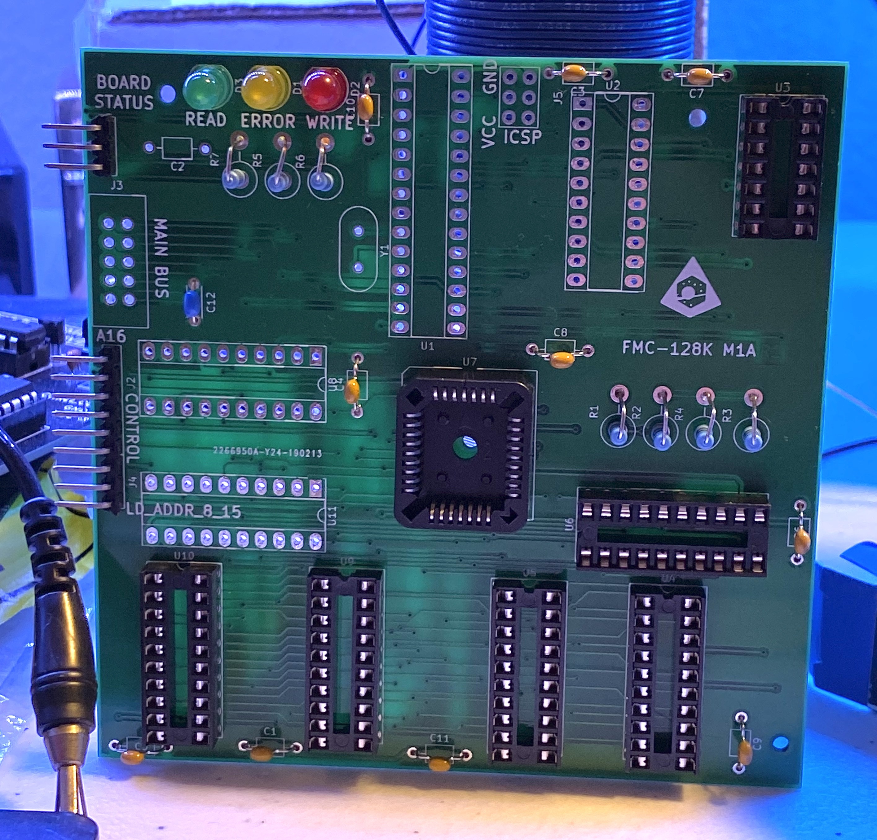
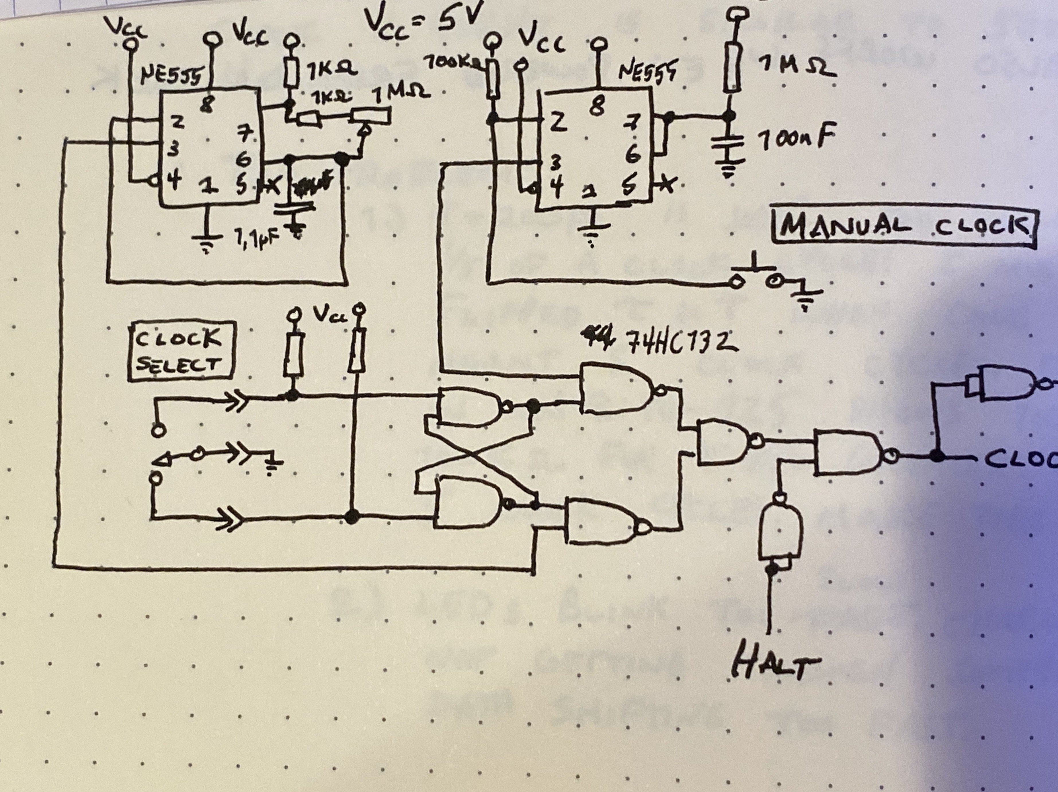
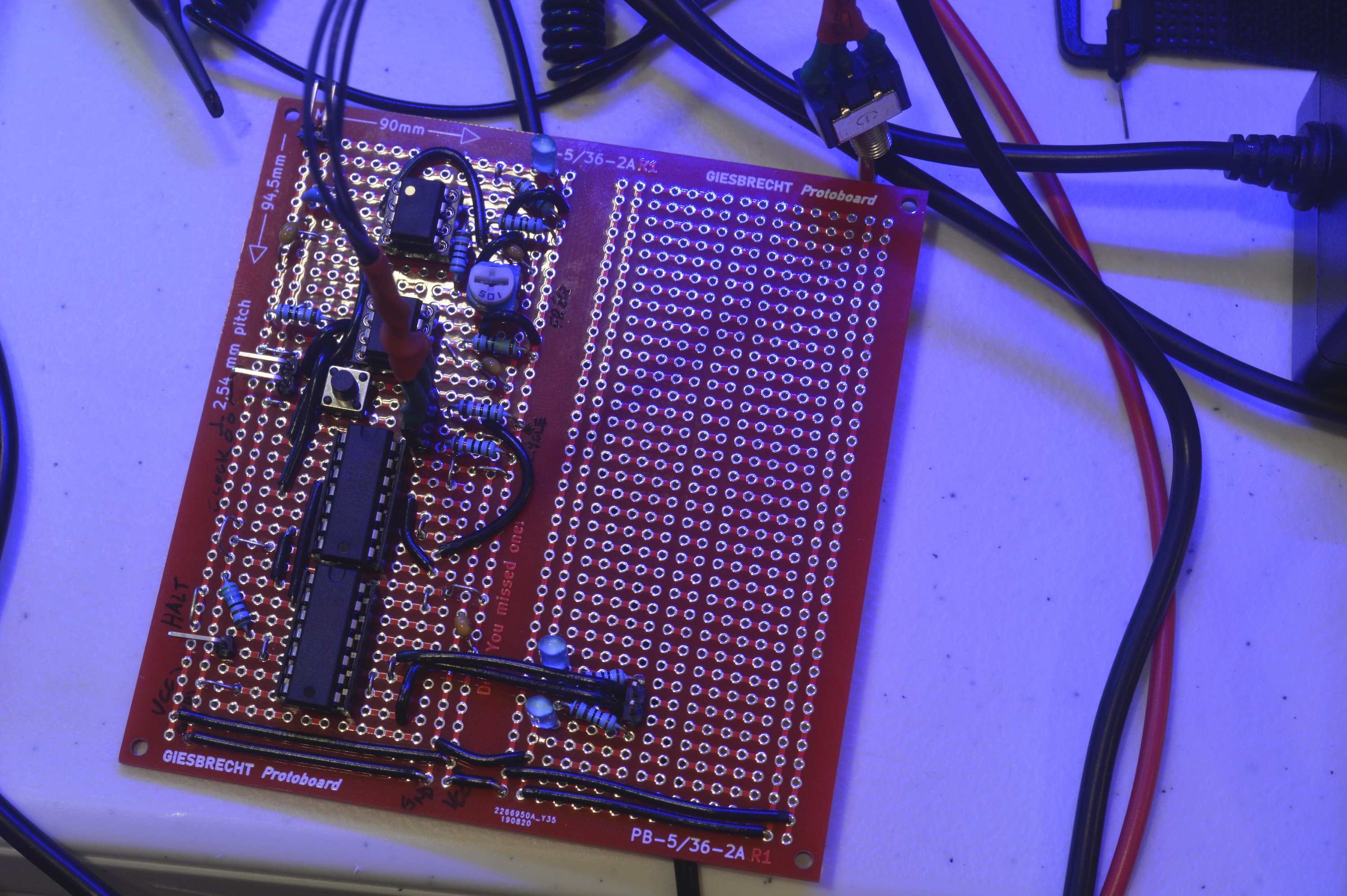
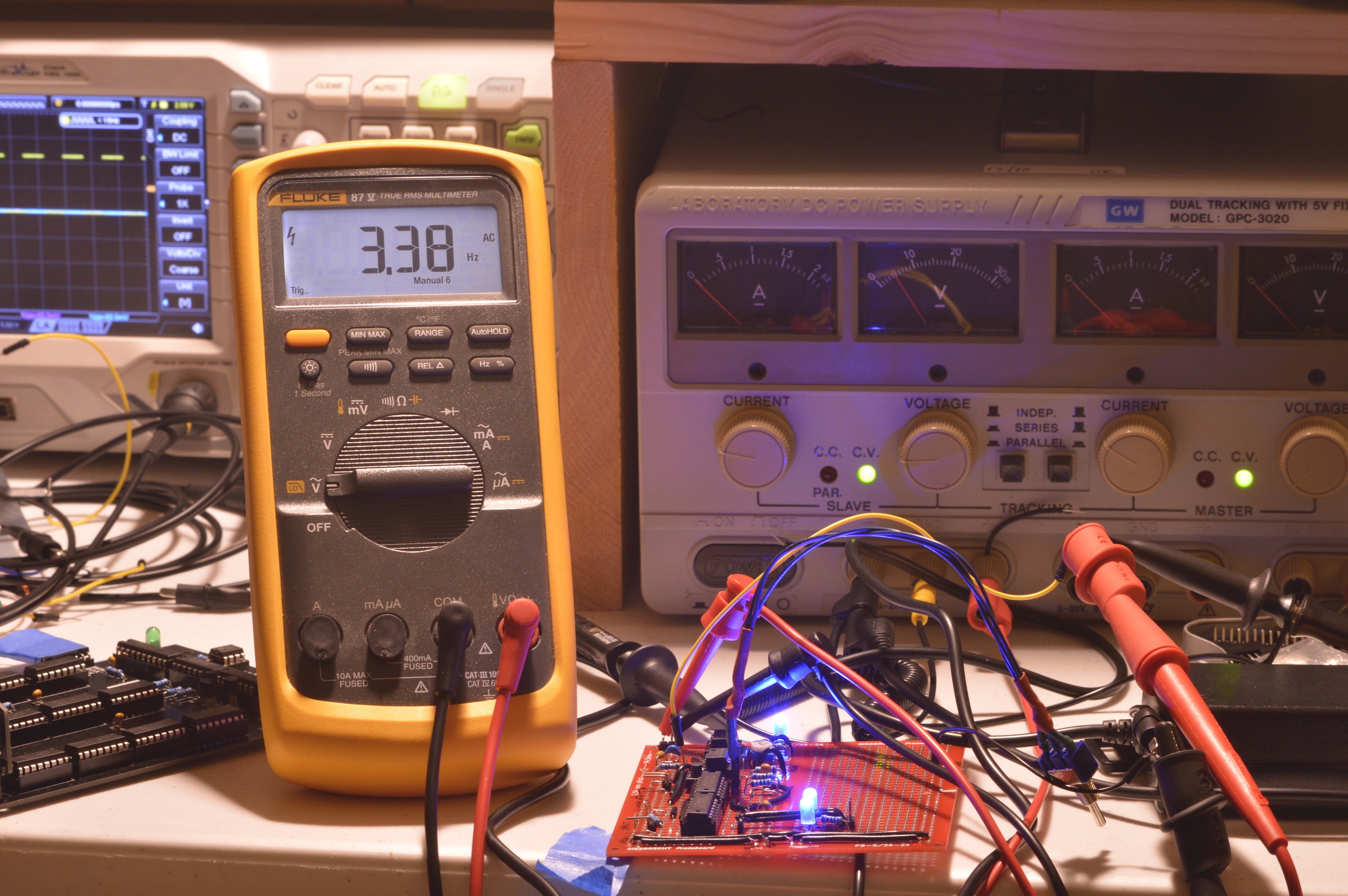
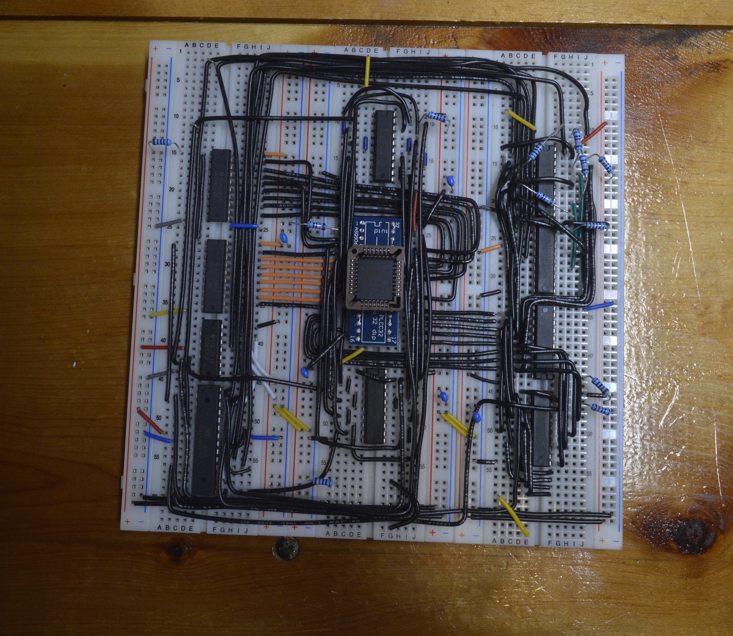
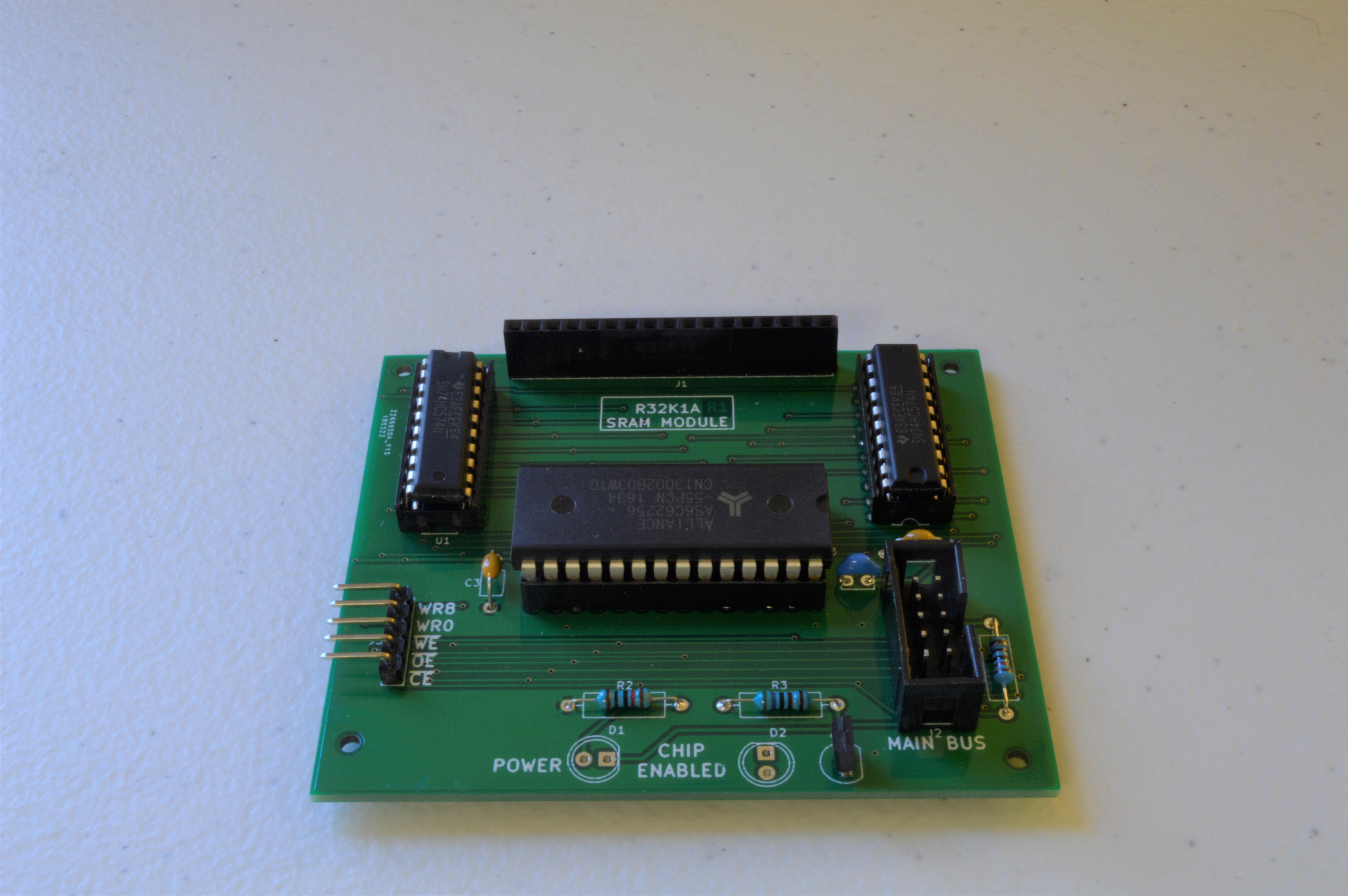
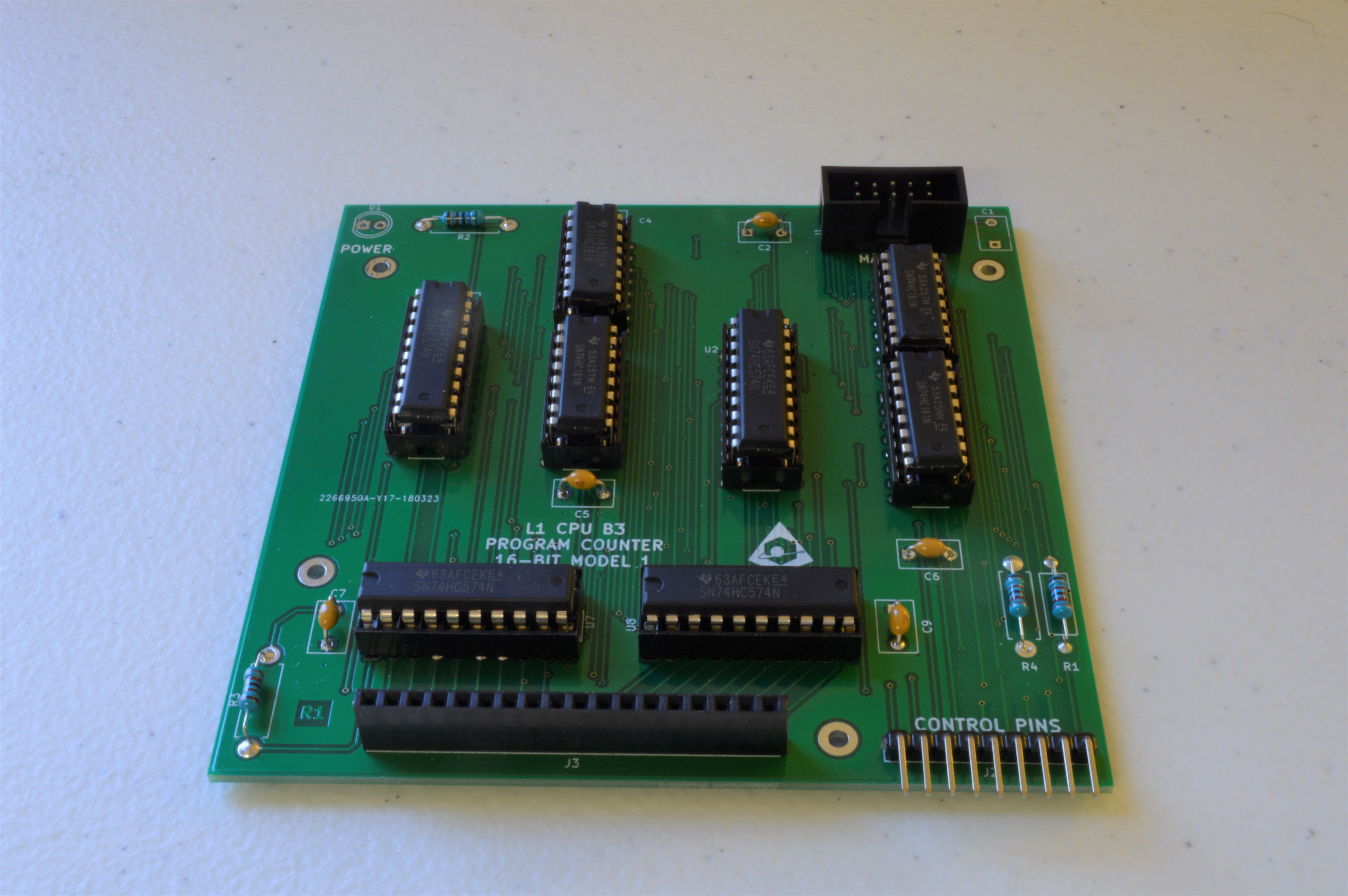
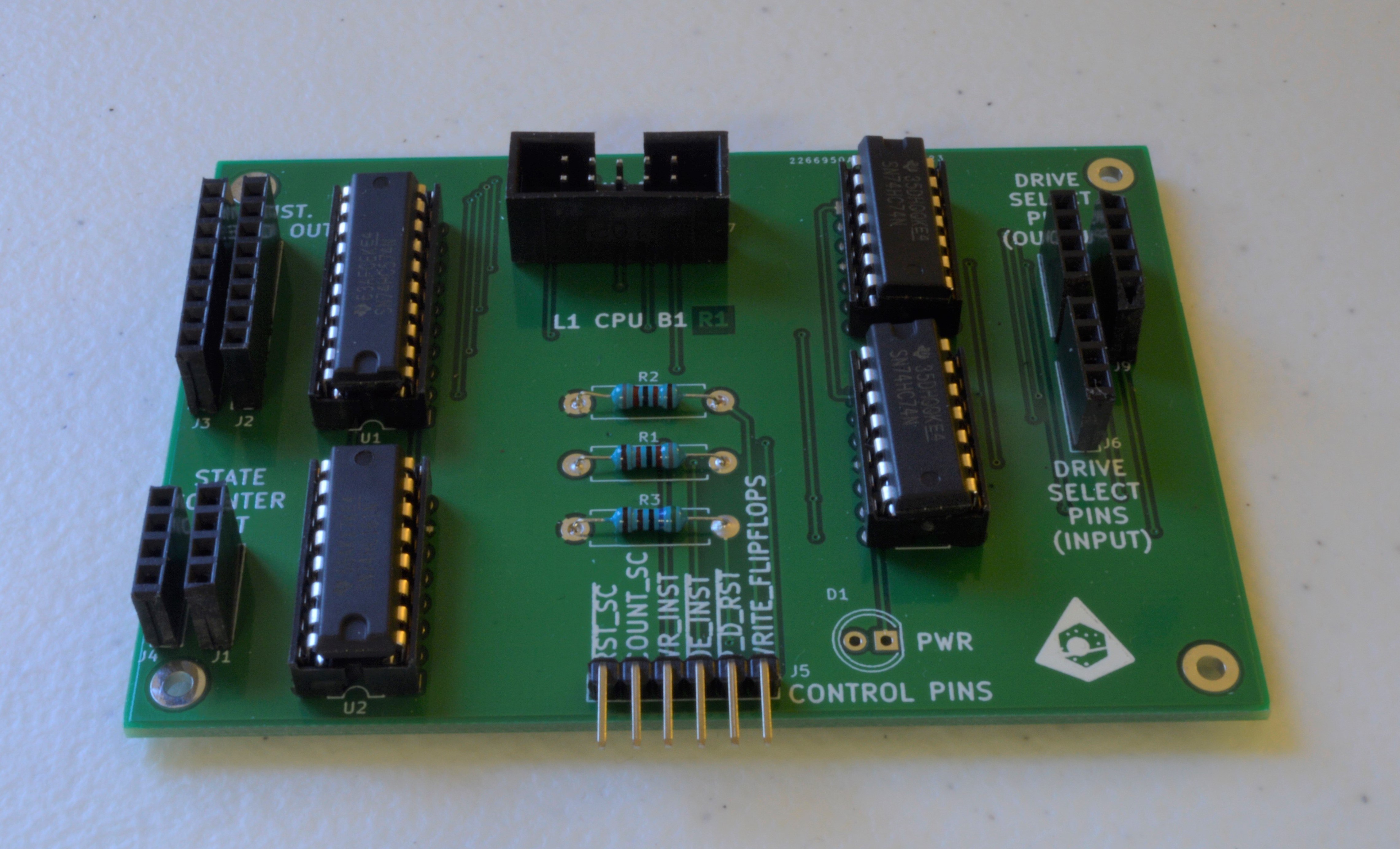
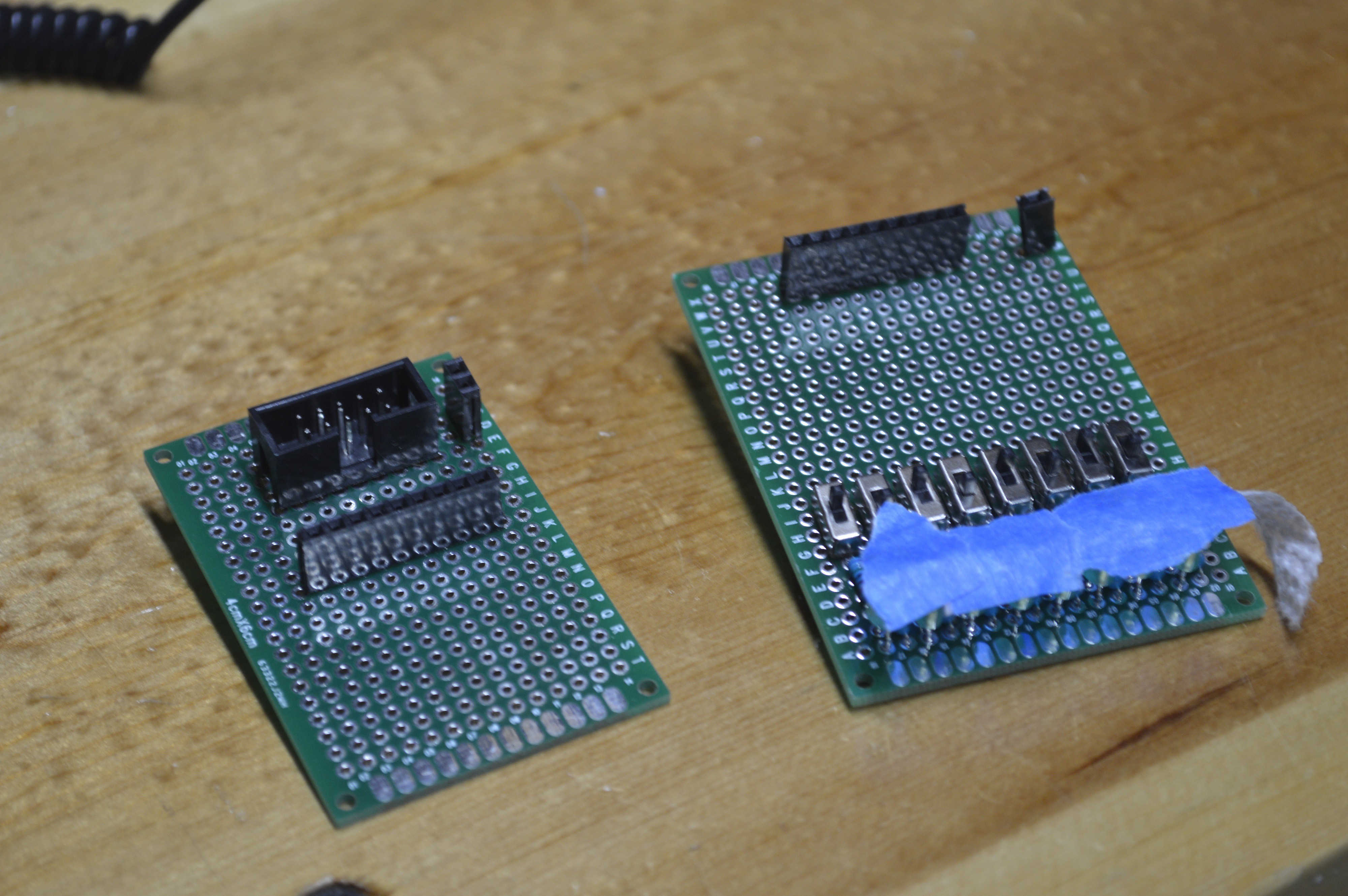
The computer has been designed and PCBs are here! I'm currently soldering everything together (as of summer 2021) and hope to have everything ready to test by the end of August! I'll be posting updates as I get modules completed.
0%
0%
Blinkenrechner
Computer based on a homemade 8-bit CPU
Become a Hackaday.io member
Already have an account? Log in.
Just one more thing
To make the experience fit your profile, pick a username and tell us what interests you.
Pick an awesome username
hackaday.io/
Your profile's URL: hackaday.io/username. Max 25 alphanumeric characters.
Pick a few interests
Projects that share your interests
People that share your interests


 Bentendo64
 Benchoff
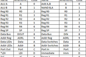
 agp.cooper
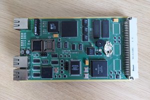
 Tom
Tom
Awesome. Looking forward to you updates =)