 Richie Ellingham
-
Tearsday Thurdown #5
08/19/2023 at 04:03 • 0 commentsThe Involuntary Teardown of the WF-1000XM4 Charging Case
I was cycling back home from a Saturday brunch blasting the funky audio waves of Franc Moody through my best earphones to date, the Sony WF-1000XM4 earbuds. I got home and performed the ritualistic wallet, keys, phone, earbud case pocket haka. There was no earbud case present in my pocket. I retraced my steps and sure enough they had fallen out of my pocket in the middle of an intersection whilst cycling. Sure enough the form factor was now very slimline and design somewhat minimalistic with all parts having been cold rolled several times by the local neighbourhood SUVs. Here’s a great indepth teardown: https://www.qucox.com/sony-wf-1000xm4-teardown/. The housing was completely jodido (fucked), so this will be brief.
The Housing
The outside of the case was a premium matte black plastic with a glossed plastic on the inside. The assembly of the all the components during use was very snug, with that solid dense feeling even though much of the plastic wall used was very thin <1mm. A piece of foam was embedded in the plastic to ensure the battery was safe from any impacts or the ever dreaded Lipo swelling. There were three magnets recovered (out an assumed total of four). These were extremely strong and had gathered many of the SMD components during the cold rolling process of the charging case. Likely neodymium, n52 grade.
The Circuitry
The circuitry was also jodido, so the only things of note we can see are the custom induction charging coil, the charging USB C port and the small 520mAh single cell Li-ion. Also there was a flexible ferromagnetic material inbetween the battery and the copper coil, to redirect/sink the magnetic field coming from the wireless charging emitter. Here’s an interesting article about electromagnetic lensing of radiowaves using a ferrite core: https://en.wikipedia.org/wiki/Ferrite_core#Ferrite-rod-aerial
As for the earbuds, these are by far the best noise cancelling earbuds I have ever tried with a sound quality that’s hard to match with any other earbud.
-
Tearsday Thurdown #4
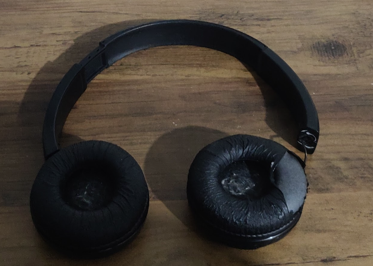
05/12/2022 at 08:41 • 0 commentsTearing into Sony WH-CH510 headphones
These headphones were stolen off a friend who had owned them for many years as he was going to throw them out. Why were they bin worthy? A piece of plastic snapped on one headphone, which I was able to fix with a bit of super glue. These are still in great working condition even with the thoroughly worn ear cushions.
Housing
The mechanical design of the headphones are simple the plastic curved piece of plastic has a good amount of spring to hold the headphones over a large head and could be adjusted with a sliding mechanism with multiple soft locking notches. The headphones are very lightweight so let’s open them up to see what’s inside.
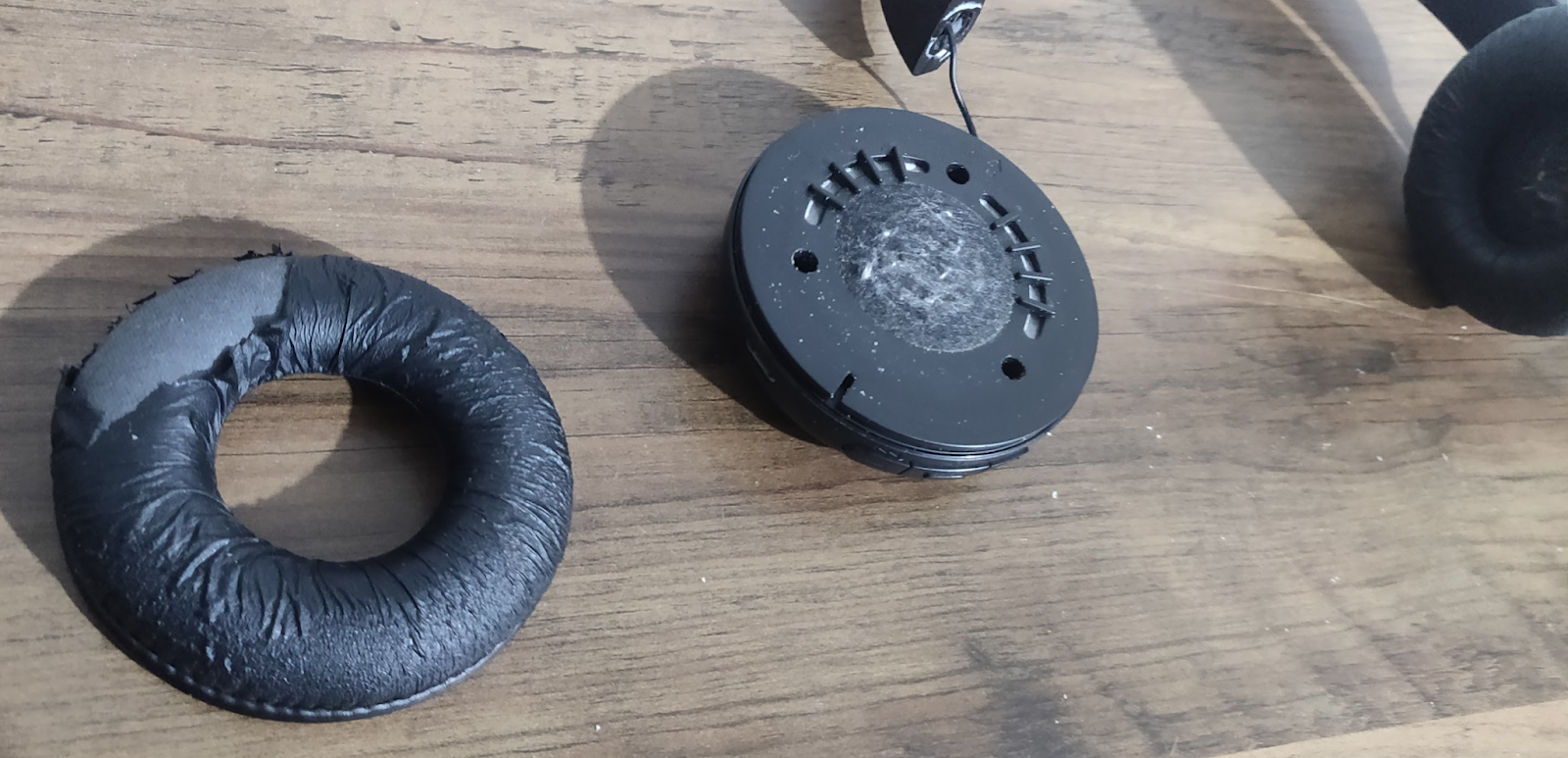
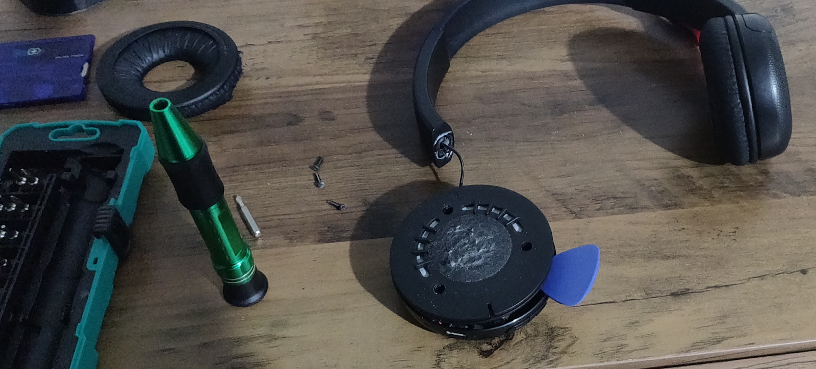
The first step is to remove the ear cushions from the headphones, which exposes three screw holes.Once the screws in these three holes have been removed you can proceed to separate this plastic plate, by levering a small flathead screwdriver into the bottom, where there is a notch in the plastic plate. Now we can see inside the headphones!
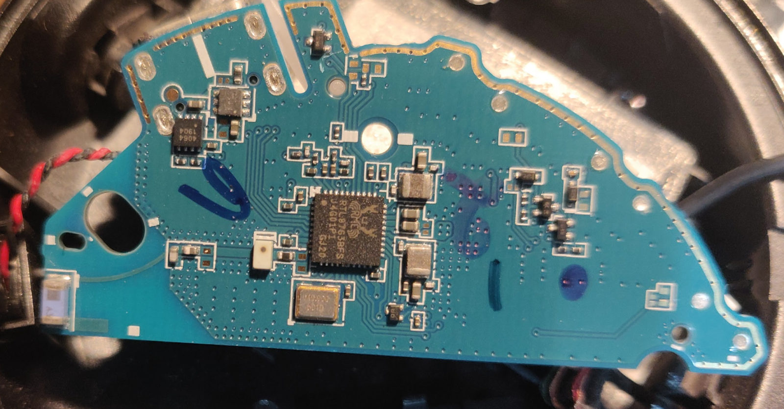
To the electron city! (aka PCB)
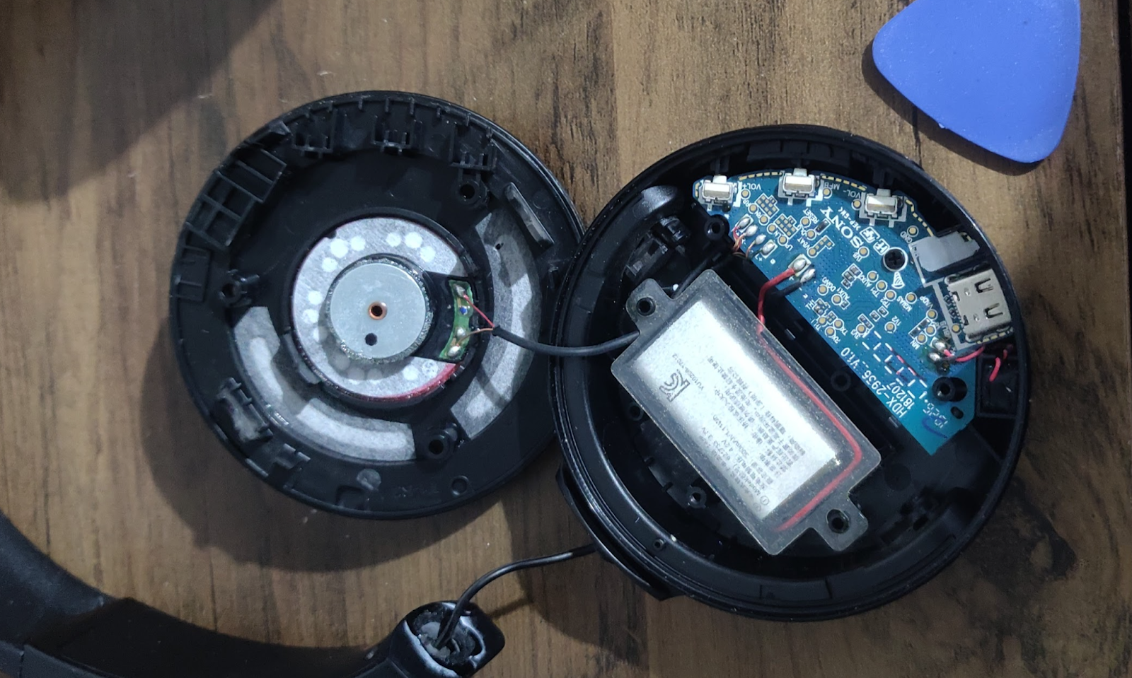
All of the circuitry for this device is located in the right headphone housing as seen below. This circuit is very simple and has similar components to my first teardown of some wireless earbuds. However these headphones have a much larger volume of space, sizing constraints are much less of an issue (boring!). The major components we can see when we open the housing is a 3.7 V Lipo battery, a small conical speaker and the main PCB.
On the circumference of the PCB from left to right we have three tactile switches and LED connected to a lightpipe and a USB C charging port. The top of the PCB has very few components; only passive components like resistors, capacitors, and test points are present on this side. We call also see ‘through via’ stitching throughout the board to shield the RF parts of the circuit and ensure impedances of radio frequency lines are controlled. To reveal the other side of the PCB we simply unscrew one black screw near the centre of the PCB.
The rear of the PCB is also very simple. We have the power management circuit next to the USB header, the micro in the centre of the board and what looks like some FETs, diodes and maybe a regulator sparsely scattered around the rest of the board. The crab logo is a clear indicator that this is a Realtek SoC (RTL8763BFS). This SoC contains a silly amount of features including:
- Low power DSP - dedicated filtering microphone data and a 24bit audio codec
- Integrated dual switch mode power regulator, linear regulators, and battery charger; charging current up to 400mA
- Bluetooth radio - BLE, BT 5.0 and BDR/EDR
- USB 2.0 and USB C compatibility
- 32-bit ARM Cortex-M4F Processor
Amongst many other features somehow packed into one small package.
Below the SoC we can see a 40MHz crystal oscillator. Surrounding the SoC in close proximity are of course the decoupling/bulk capacitors.
To the left of the PCB we have an PCB trace antenna which will have all of its trace and components specifically sized to a specific impedance to optimise the radiation power of the antenna. There seems to be a blue multilayer chip antenna of sorts attached to the end of the PCB trace antenna. It is difficult to know how this antenna setup works without learning more about the intricacies of antenna engineering and the relevant electromagnetic physics principles. This is meant to be a good site for mere laymen who want to learn about antennae from fundamentals -> https://www.antenna-theory.com/ .
Conclusion
Overall a very simple teardown with proof that complex circuitry isn’t required at all when you can find a SoC that can do it all from power management to radio to processing etc. A fun quick easy teardown. They worked perfectly when put back together ready to push more well timed air pressure waves into my ears!
-
Tearsday Thurdown #3
04/21/2022 at 09:40 • 0 commentsGarmin Vivoactive 1 teardown
I’ve had this Garmin Vivoactive for over 6 years now and upgraded a couple of years ago to the Garmin Forerunner 45 for running and swimming. The old Vivoactive used to have the stamina of a rabbit in bed (it had a great battery life), but the battery life rapidly deteriorated as I was starting to use it a lot less. The watch strap completely broke on one side so I replaced it with a piece of janky elastic. It still functions well, taking a reasonable amount of time to pick up some solid GPS satellite signals. Enough chit chat let’s tear in!
How do we open a waterproof watch??
The housing of the Vivoactive is very sleek and much thinner than many other current smart watches(8mm vs 12mm for my Forerunner 45), but also has much less features. After a good few minutes of inspecting the watch for any edges to pry open I noticed a change of material between the watch face and housing. I assumed like in other devices (such as phones and the Kaiser Baas teardown that the screen was simply glued on. Being a water-tight device my smallest tools could not pry the screen off, so I use an iron to soften the glue holding the screen down. I then used a small suction cup to pull on the screen, which lifted a small edge to be pryed open as seen in the figure below. This has definitely ruined the original 5 ATM waterproof rating of the watch.
The insides
After very carefully prying off the LCD/touchscreen the quite simple insides were exposed. The main visible components were the
- Lipo battery, 150mAh, 3.7v
- PCB
- Antenna
- Flex PCB interconnect
The antenna is made by TE and sits on three pins protruding from the PCB. A small connector sits under the antenna, which could be used for programming or other testing purposes. The push buttons on either side of the PCB are supported with a resin substance. The main IC seen on the right side of the PCB is a Nordic nRF51422 BLE, ANT and 2.4 GHz SoC. A great SoC for a wearable device, with plenty of computing power with its M0 core, flexible radio usage, and low energy modes. There is an external 32MHz crystal oscillator adjacent to and driving the Nordic chip.
In the centre of the PCB we can see a low profile FPC connector. All of the the components look to be 0201 as expected with a wearable device of this size. There is a farm of caps and resistors on the left side of the PCB likely a mixture of decoupling caps and peripheral components for setting up IC parameters.
The dark side of the PCB
To access the other side of the PCB the LiPo battery is gently levered out and the four conductive ‘power’ screws are removed. Upon removal and flipping over the PCB we find that the other side is completely boxed in and shielded. Half of the metal shield is covered in copper tape with the other half of the laying under the battery. Under this side we likely have an IMU, a GPS module and adjoining circuitry.
The antenna is provided by TE connectivity and has a PN that looks like 2??8462. To aid the rf part of the PCB we have a keepout copper area between the antenna and the SoC. There is a component between the antenna and the SoC which is likely to be some kind of impedance matching/ signal conditioning circuit. We can also see ground plane stitching around the perimeter of the PCB, in particular near the antenna. There are many exposed circular gold plated test points
on the PCB, likely for use with an ICT method like flying probe or bed-of-nails.
The screen used for the watch uses memory in pixel (MIP) technology where the LCD pixels required a very low power to stay ON. This is evident as the screen does not emit light but uses ambient light to illuminate the screen or a backlight on demand. The screen is also a touch screen for extra UI functionality.
The charging case
The charging case was simple to pull apart, only held together with glue. There is a single component PCB in the case with a 2A fused attached to the positive...
Read more »


 Lutetium
 Carl Bugeja
 ekaggrat singh kalsi
 Curt White
 Kn/vD
Kn/vD Frédéric Druppel
 Will Donaldson