 Eric Hertz
#sdramThing4.5 "Logic Analyzer" has quite a bit of info regarding the core concepts of what I've coined "Free-Running" SDRAM... The basic idea is to connect the SDRAM's command/address pins directly to (some of) its data pins. Doing-so, then, allows you to load up the memory-locations with commands/addresses to be sent *back* to the memory itself. Then, it's possible to completely remove the SDRAM from a controller. Again, that has been described somewhat thoroughly (including a video of the SDRAM sampling/repeating data without a controller) at the link, above.
Here's a few schematics from that project. They might get modified slightly for this project, but probably not much.
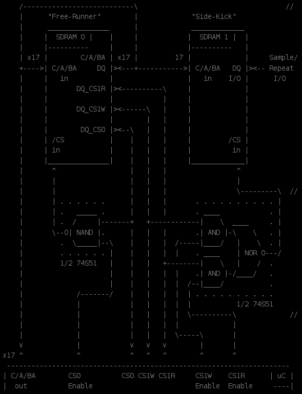
Here you can clearly see how the Command/Address/Bank-Address pins are directly wired to Data I/Os on the same "Free Runner" [group of] chips.
Note that SDRAM DIMMs have all chips' C/A/BA pins tied together, but each chip can be selected via various combinations of Chip-Select, and Data Masks (not shown, above).
Also shown in this schematic is the means for allowing the "Side-Kick" to pay attention to an entirely different set of commands than the "Free-Runner". This is accomplished by multiplexing the chip-select DATA I/Os between the two devices. All commands are sent to all chips, but only those that contain the proper Chip-Select (output from the data I/O and routed through the multiplexing-logic) are actually paid attention to.
So, again, the Free-Runner might automatically iterate through each page of memory, outputting its entire contents (and in so doing, paying attention to its contents *as commands* to continue iterating through its contents). At the same time, those contents might contain commands for the "Side-Kick" that tell it to either *sample* data at its I/Os (an SDRAM-Write command), or to "repeat" data (an SDRAM-Read command). Again, all those commands are sent all the time, but only those selected by the multiplexer cause an appropriate Chip-Select for the Side-Kick.
In a sense, once the free-runner is loaded with all its data/commands, it then acts *as* the controller for [both itself and] the side-kick. The side-kick, then, is pretty much the "memory" we're interested in reading/writing from/to, which would then contain the samples from a logic-analysis sense.
In order to communicate between the SDRAM running at a much faster speed than the processor, sdramThing4.5 made use of one-shot circuitry, as shown below:
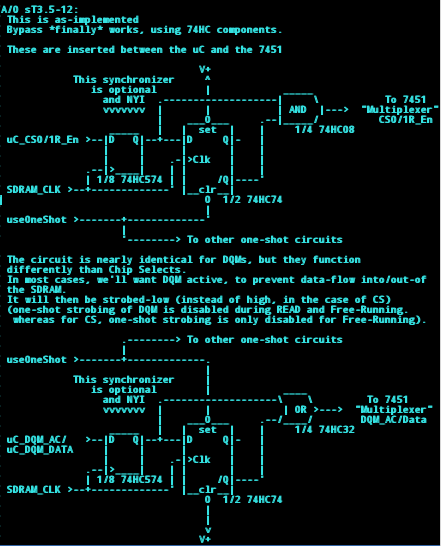
The basic idea is that, say, a rising-edge output by the controller (e.g. an AVR or RPi GPIO) would result in a single pulse at the output of the one-shot circuit. This is necessary in order to assure that the SDRAM receives commands/data [written by the slower processor] only once, in one single (faster) SDRAM-clock-cycle.
(TODO: WTF? "To 7451 'Multiplexer' DQM_AC/Data"... No, those aren't muxed, right?!)
In sdramThing4.5, *several* one-shot circuits were necessary. However, discovery of the CKE (clock-enable) input's functionality--and SDRAM's ability to be arbitrarily halted via that pin--could very well whittle that down to a single one-shot circuit. Awesome.
FURTHER, using this method would allow for *completely arbitrary* timing on the command/address/data pins, such that even a *really slow* processor could load each byte in its own time with no specific timing requirements. Thus, interrupts could be running, or in the case of a single-board-computer where the timing is imprecise due to OS overhead and memory-caching, etc. there's no worry about keeping the timing of its GPIOs perfectly precise. In sdramThing4.5, on the other hand, it was absolutely necessary to know exactly how many clock cycles it took between the changing of pins. This CKE thing will make the entire process *considerably* easier, and open new doors as far as what types of software (no longer limited to Assembly!) and hardware it can be interfaced with. Thus, sdramThingZero's being a bit more of a peripheral, independent of a specific processor, rather'n a complete system (as sdramThing4.5 was).
Here's a picture of sdramThing4.5:
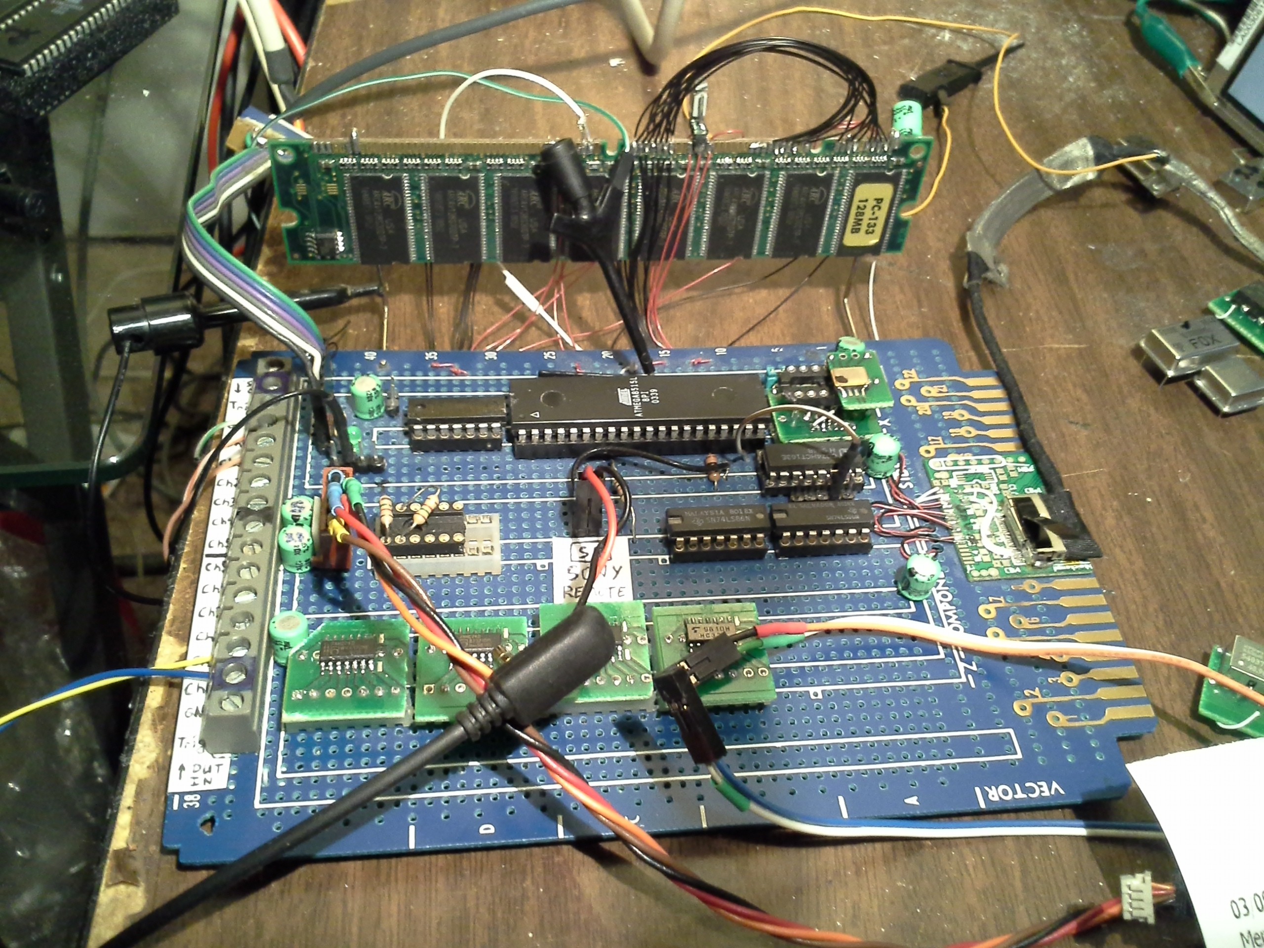 The surface-mount boards near the bottom (four chips) are used for one-shots. These were added in a late prototyping stage, so were not part of the original design. They introduce tremendous delays and noise, due to the ratsnest of wires below the board, and due to extending signals away from the processor *and* the SDRAM, before extending them *back*. So, obviously, having a PCB designed for the purpose would probably speed things up quite a bit. Further, again, we'd only need one (maybe two) of these circuits, instead of several, which would reduce problems with delays, etc. as well. I'd say it's entirely feasible to get it running at the full 133MHz (That'd be 133MS/s for a logic analyzer) with a new PCB and using CKE-one-shotting.
(You can also clearly see in the picture how the command/address pins are directly wired-back to data-pins)
Here's some data sampled with sdramThing4.5
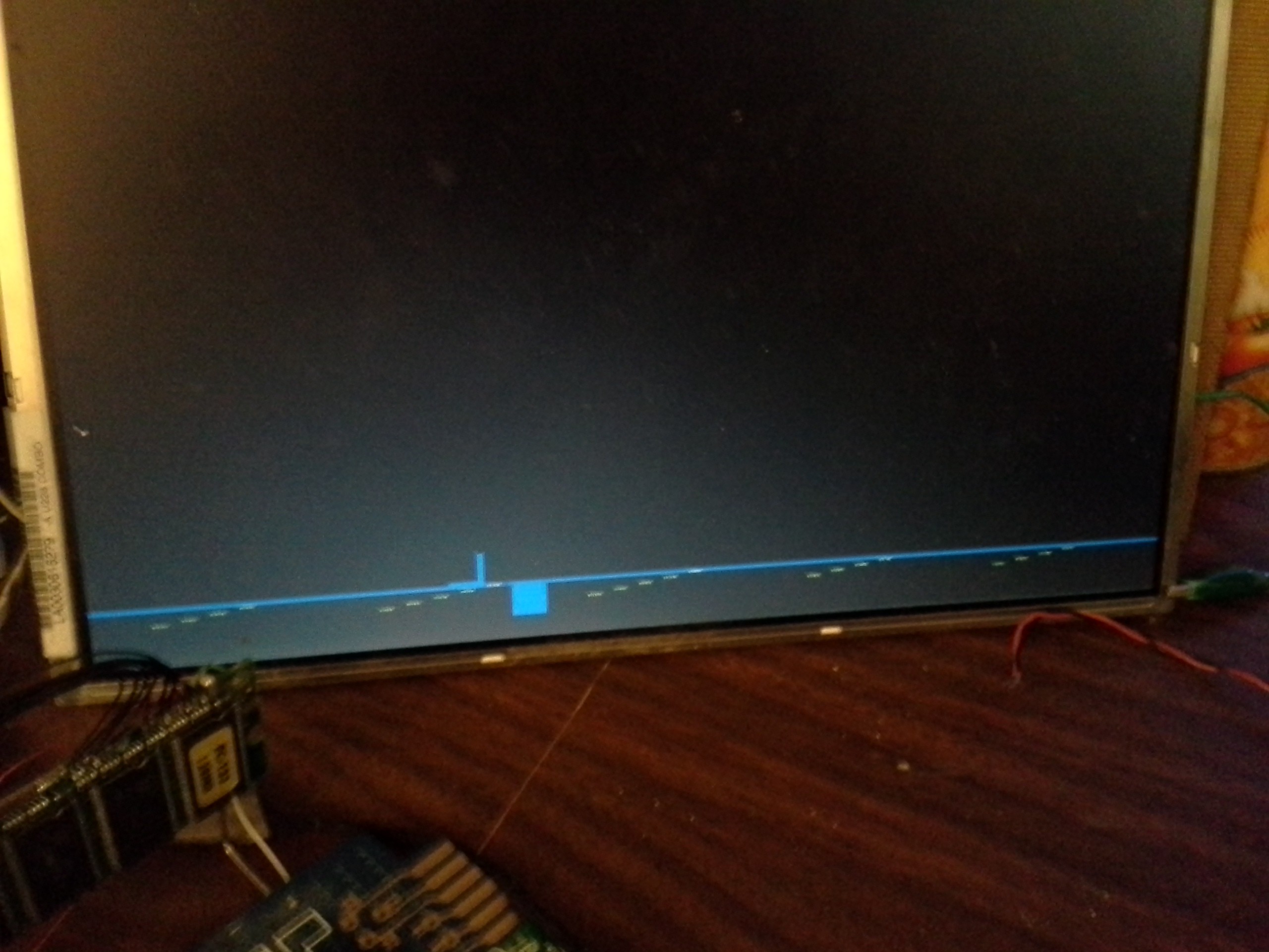
The stair-step pattern is data sampled from a SPI communication with a motor-driver (protocol-unknown at that point). (The blue lines are cursors).
Unlike sdramThing4.5, sdramThingZero would *not* have a dedicated display. The display would be supplied by the computer, and the user-interface would be a piece of software which could render these samples as regular ol' timing-diagrams which could be scrolled through, etc. and would be much more visually-intuitive.
Similarly, sdramThing4.5 is a "sample/repeat" "logic-analyzer" which means it samples a data-set, then repeats that same data-set to its same pins. Thus, in order to "see" the waveforms, it was necessary to connect those data-pins to an oscilloscope. sdramThingZero needn't be limited to sample/repeat. Instead, it would sample the data, then the controlling computer would transfer that data-set into its own memory wherein any sort of visualizing/processing could be done.
So far, sdramThingZero is still in the concept-phase. I'm darn-near-certain this CKE thing will render it doable, to say the least. (Whereas before I discovered the CKE thing, I thought it darned-near impossible to interface with the SDRAM without *very* specific timing not available from computer GPIOs).
The main limitations are the need for a tremendous number of buffers and latches in order to reduce the pin-count to something reasonable for a non-dedicated controller. Thoughts on FPGAs or CPLDs have definitely gone through the ol' noggin', but I don't think them appropriate for the goals of this somewhat obscure (but potentially quite-useful) project to be accessible to those with limited tools and knowledge. So, a lot of buffers/latches might just be where this goes.
Discussions
Become a Hackaday.io Member
Create an account to leave a comment. Already have an account? Log In.