 Eric Hertz
Writing up the last log got me thinking about some things...
I'm not sure why, but for some reason it seems significantly simpler to handle data-routing down to an 8-bit interface now than the last time I looked into it (a couple logs back). Maybe I'm forgetting something... but here's what I've come up with:
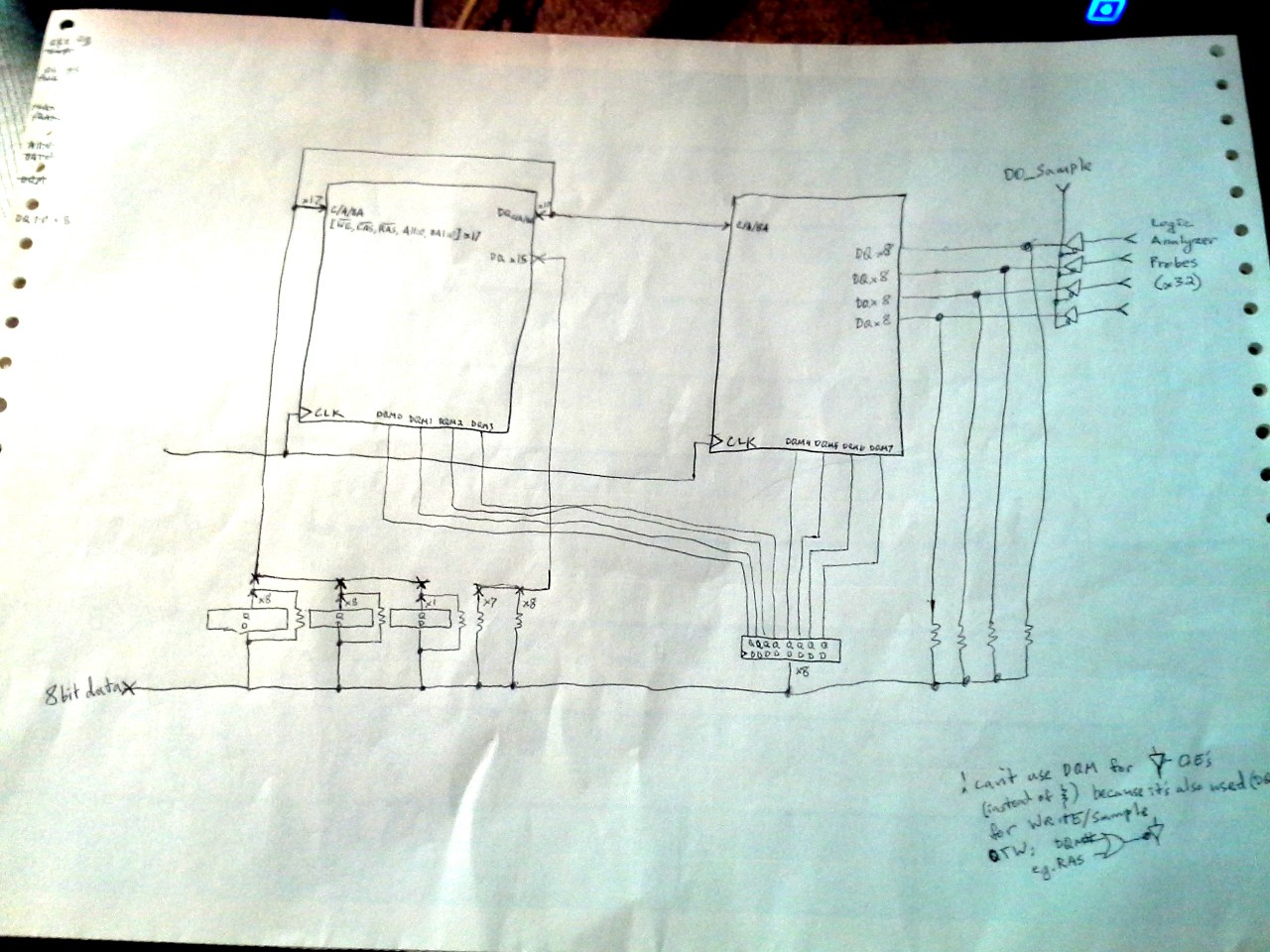
So, actually, it's not that many components. For some reason I thought I needed latches for every DQ-byte, but I think with proper timing of the DQMs that's almost completely unnecessary. I think the only latches necessary are for the Command/Address inputs. And, removal of a shitton of buffers with output-enables can be accomplished with resistors, instead.
One KEY-factor in this reduction is moving buffers to the probe-inputs... This is something I wanted to do, anyhow, as having them allows for e.g. using 74AHC244's, which would allow for sampling 5V levels, as well as 3.3V.
So, I think, there's a necessity of only 8 glue-logic chips: (4) 74xx574 latches and (4) 74xx244 buffers. There will, OTOH, be a necessity for 64 resistors, which of course could be network-resistors. I'm thinking 1k should work fine without slowing things down much (if at all) due to the necessity to overcome input-capacitances.
So, the key, I guess, is that using resistors allows for bidirectional flow, whereas I think the more-appropriate method (e.g. on an actual data-bus in a professional product) would require e.g. 74xx245s and switching of the directions and output-enables as appropriate (which would require a LOT of additional control-signals!)
So, again, I don't know why I didn't see it before, it seems blatantly obvious now... So maybe I'm forgetting something.
-------
This schematic doesn't show the one-shot circuits necessary. I'd been thinking I'd need only one for CKE, but it turns out I'll most-likely need another (on the chip-select input) because I think CKE is specific to certain commands (e.g. pausing a burst-read) and might not work with single-cycle commands like "Load Mode Register." Still, there's the benefit over the last system in that only one one-shot need be used at a time.
And, I think I can make use of some of those additional latches in the third chip for other command-related purposes, should I think of any.
So, in all, I think I could probably get away with something like an 8-bit data/command bus, and a few additional (maybe only/less-than three?!) pins for directing traffic and strobing... So, like... it'd look a bit like a regular ol' uC bus-attached device like a Hitachi LCD, and could probably even interface to a PC's parallel port.
Discussions
Become a Hackaday.io Member
Create an account to leave a comment. Already have an account? Log In.
Your 1K resistor might be on the high side.
133MHz means 7.5ns sampling period. RC time constant for 1K and 20pF is around 20ns. (assuming 5pF for SDRAM chip and 15pF for the module/routing)
Moving the input buffers to the probe side is a good idea as it will give you the best signal quality. It is similar to old FET probes where the input signals will see less of the capacitance/stub.
Are you sure? yes | no
Briefly, those resistors are intended only for read/write to/from the GPIO "bus" which typically is quite a bit slower than 133MHz. (E.G. I saw a site claiming the RPi can get toggle-rates up to 50MHz, doing *nothing else*). Though they may slow it even further than the GPIOs are capable. That is a good point I hadn't really considered. That, thankfully, could be handled in software, by merely adding delays.
Thankfully, I think, the design is such that they shouldn't be a limiting-factor as far as *sample*-rate. That would be limited, I guess, by the rate at which the command/address DQ's can "fan out" to all (8) of the associated command/address inputs. Which is something else I hadn't considered.
And, something I haven't really *mentioned* is that read-back of those 64MB of samples into an SBC's main memory could take on the order of tens of seconds, maybe even minutes... This isn't intended to be a replacement for a quality Logic Analyzer... It's more of a hack that could be useful to others.
Are you sure? yes | no
Another benefit of having 32-bits AND buffered-inputs... It's plausible to e.g. sample whether the inputs are high/low in various Vih/Vil requirements... E.G. have each 8-bit buffer chip running on a different voltage-level (1.2V LVTTL, 2.8V, 3.3V, and 5V), then tie each "bit-probe" to the corresponding bit on all of the buffers. In a sense, a 2-bit 8-channel ADC... The list goes on, detect floating inputs/Hi-Z...? And it certainly would be a small step to connect actual ADCs to the probe-inputs.... wherein it becomes *quite* handy to have this as a peripheral to a [single-board] computer, with its processing/display power and ease of GUI software-configuration/modification.
Are you sure? yes | no
Actually, I think I can remove another latch... 8-bits of the command/address information could be on the GPIOs at the time the command is read, and no data (needs) to be available, even for write, at that time (when using DQMs) so 7 chips total for data-routing. Whoa. I think I had something like 28 in mind, in an earlier log-entry. If I could wrap my head around throwing one of those command/address bits on another pin, separate from the 8-bit "bus" I could remove another latch, as well... hmmmmm
Are you sure? yes | no