 Eric Hertz
(Can you tell I finally hooked up the ol' scanner?)
Here's a look, again, at the full schematic, currently attached to an AVR.
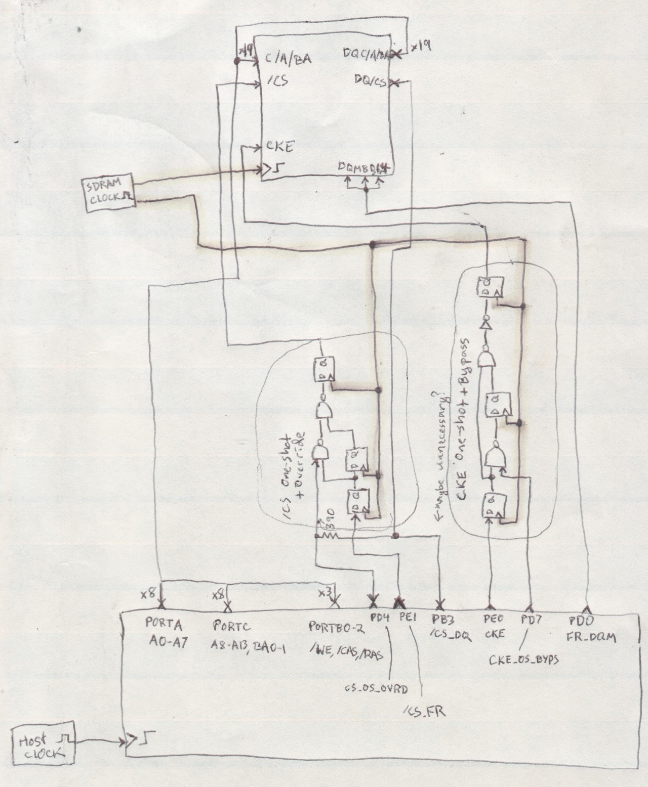
That's already 25 GPIOs just to get free-running going. (And we'll need 32 more for the side-kick's logic-analyzer-sample-data to be read-back... but that's another story, we'll come back to).
Suffice to say, that's a *lot* of GPIOs, and doesn't lend itself well to interfacing with, e.g., a RPi. Thus, I'm working on putting most (all?) of those signals on a bus... possibly 8-bits wide.
The obvious solution is to use a bunch of (bidirectional?) latches, as can be seen below.
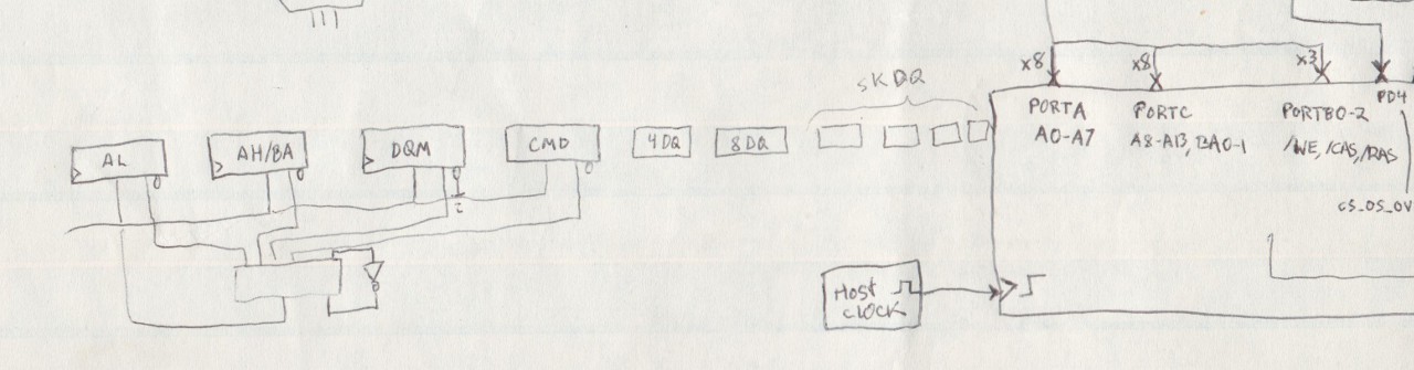
But, sheesh, do I see correctly, I'd need something like 10 8-bit latches to make this work?! Yikes.
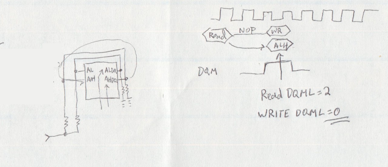
Then I had an idea... We've already got an SDRAM with fed-back DQs... those DQs are *directly* wired, already, to the Address-lines for free-running mode... I wonder if I can use that to set up an address for regular-ol writes...
By which I mean... The entirety of the Free-Runner half of the SDRAM has to be loaded with Free-Running commands, via Write, at "boot"... That's a lot of writes before free-running can do its thing.
But, check this out... Maybe I can use the Free-Runner's inherent fed-back signals for a sort of "pre-boot", which might allow me to remove TWO 8-bit (bidirectional?) latches
(This is *VERY* early-thinking... Just looking at it now I see E.G. I've got a voltage-divider scenario which could cause problems)
Well, the idea is... maybe I could load the address I want to access *into* the very first memory-location...
- Activate a row (leaving the address-lines High-Z, so they're pulled-down by the resistors, thus activating Row 0)
- Set up the DQM bits to not allow any writing to any bytes
- Start a burst-write (again, leaving the address-lines High-Z, thus beginning the write at column 0)
- Pause the burst-write via CKE, immediately upon start of the write-burst
- Set up the DQM bits to allow writing to the ADDRL_DQs
- Set up the Low byte of the desired address to the *shared* 8-bit bus
- Strobe CKE (writing the low address-bits at column 1)
- Repeat 2-7 for the High address-bits
- Start a burst-read (again, leaving the address-lines High-Z, thus beginning the read at column 0)
- Immediately pause
- Set up the DQM bits to allow BOTH the ADDRL_DQs and the ADDRH_DQs to output
- Strobe CKE 3 times
- Now the Address DQs, and thus the Address *inputs* have on them whatever you set up previously.
Apparently this is where I haven't thought the whole thing through... The key-factor, I thought, while drawing this, was that Read has a different DQM-Latency than Write. This goes against all the timing-diagrams shown in data-sheets, but they probably hadn't considered a case where you might *want* read-data at the instant you're starting a write (and intentionally DQMing that first column)... SEEMS like this should work.
But...
I don't generally want to start a write-burst at a specific column address. Usually I want to start a write-burst at column 0, then load up the entire page... So, worrying, at this early stage, about following up that Read, to load the address-lines, with a Write doesn't make a huge amount of sense.
A more complicated scenario (and much more common) would be that I want to set up those address-lines to Activate a different Row... Can that be done?
Seems I'd need to keep the Bank-Address lines separate from the Address lines, driven explicitly by a register or the uC...
But, yeah, I think it can be done. (And, there's no problem performing an Activate, on one bank, while read-bursting from another... That's an inherent feature to SDRAM, and highly important in Free-Running).
Then the question becomes, can it be used for *all* cases where I need the address-lines set-up...?
And the answer is a resounding NO... If nothing else, Load-Mode-Register, which is necessary to initialize the thing, uses the address-lines as the data-inputs to the Mode-Register. Maybe I can tie those "pull-down" resistors, instead of "down", to the mode-register setting... hmmm.... So, then, instead of writing to row-0 col-0, we'd be writing to some random-ish location... but that shouldn't matter as long as whatever random-ish location that is, is both read and written... (Could program Free-Running to just skip over that page entirely).
...
And, handy, the upper address-bits in the mode-register are all written 0
So's we won't be trying to access a row/column that might not be in the SDRAM (surely all SDRAMs have at least 256 rows and 256 columns, right?) And, actually, based on the first bit that needs to be high, we'd only need at least 128 rows/cols to make this work... Awesome.
This might actually be doable! Gotta figure out what to do about those resistor-voltage-dividers...
And plausibly doable with other DQs as well... e.g. /CAS_DQ, etc....?
Discussions
Become a Hackaday.io Member
Create an account to leave a comment. Already have an account? Log In.