Here's a block diagram of the overall organisation I have in mind.
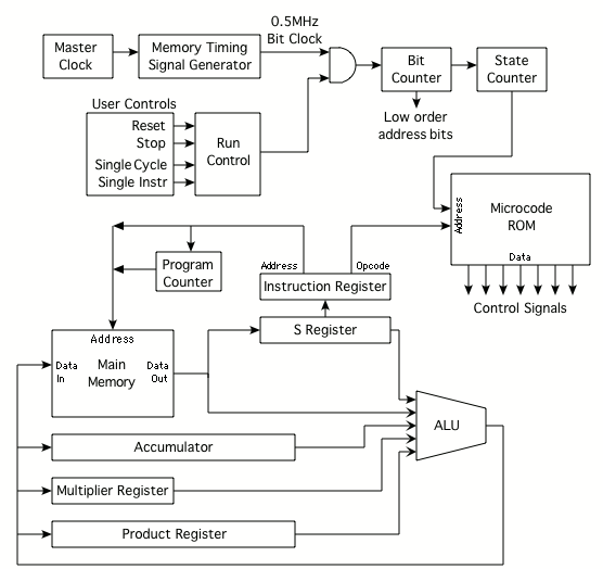
The Memory Timing circuit produces control signals for the dynamic RAM
and divides the master clock down to 0.5MHz. This is gated by the
output from the Run Control circuit to produce the bit clock for the
rest of the machine.
The Bit Counter counts from 0 to 17, representing one short word cycle.
Its output is used as the low-order address bits for both the main
memory and the memories holding the register values.
One microinstruction is executed during each short word time, after
which the State Counter is incremented to move on to the next
microinstruction (unless a microbranch causes it to be loaded with a
different value). The output of the State Counter forms the low order
bits of the microinstruction address, with the high order bits taken
from the opcode bits of the instruction being executed. I'm currently
planning on using a 4-bit state number, allowing for up to 16
microinstructions per machine instruction. This ought to be more than
enough, but it can be increased if the need arises.
The Program Counter is 10 bits wide and keeps track of the next machine
instruction to be executed. The word address for the main memory comes
from either the Program Counter or the address field of the Instruction
Register.
The S Register is a 17-bit shift register that does not have an exact
equivalent in the original machine. It performs serial-to-parallel
conversion of instructions read from main memory, and will also hold
one of the operands during a multiplication (which is why there is no
Multiplicand register in the diagram).
The Product Register did not exist in the original machine. It will be
used to build up the result of a multiplication before adding it to or
subtracting it from the accumulator.
The ALU will be capable of Add, Subtract and Logical And operations, as
well as passing one operand through unchanged or generating a constant
output of zero. Inputs can come from the main memory, the accumulator
and the S, Multiplier and Product registers. The result can be written
to the main memory, the accumulator, and the Multiplier and Product
registers.
Outputs from the Microcode ROM control the functions of all the other
parts of the machine, including loading of registers, selecting inputs
to the ALU, selecting the function performed by the ALU, and writing to
registers and memory.
I/O devices are not included on this diagram, as I haven't decided exactly how they will fit in yet.
Also not included is the system responsible for refreshing the main
memory and generating the oscilloscope displays of memory and register
contents. This will be an autonomous unit that operates entirely
independently of the computational logic.
Discussions
Become a Hackaday.io Member
Create an account to leave a comment. Already have an account? Log In.