 spudfishScott
From a functional standpoint, the only differences between the Spikeputor's Register Memory and the Register Memory of the "Beta" processor on which it is based is a decreased number of registers (8 vs. 32) and a decreased number of bits per register (16 vs. 32). Otherwise, the inputs and outputs are the same. RegMem has three register address inputs (Ra, Rb, and Rc), three bits each, a 16 bit data input (WDATA), two 16 bit outputs (RADATA and RBDATA), three control lines (RBSEL, WASEL, and WE), and a clock input.
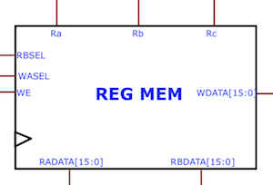
Functionally, register Ra is immediately placed on RADATA. The RBSEL signal determines whether Rb or Rc is placed on RBDATA. WASEL selects whether Rc or R6 (used as the exception pointer on IRQ) will be written to, if WE is high, on the next rising clock pulse.
The full schematic of the register memory is shown below, and includes some logic to handle the control lines, decoder logic to translate each of the address signals into enable signals for the writeback and output functions, load enable positive edge-triggered flip-flops to store the data, and tri-state buffers to select each of the two output channels.
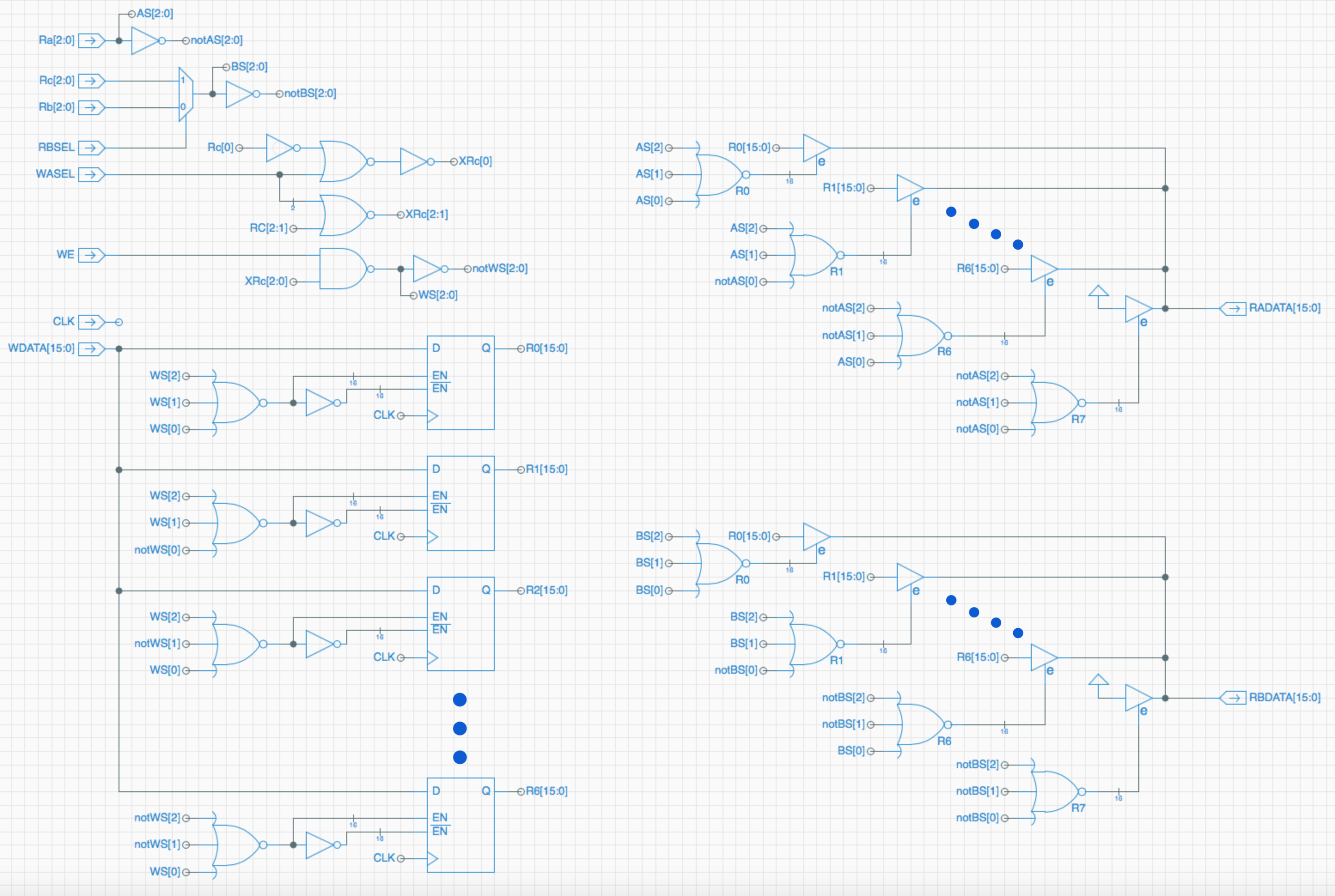
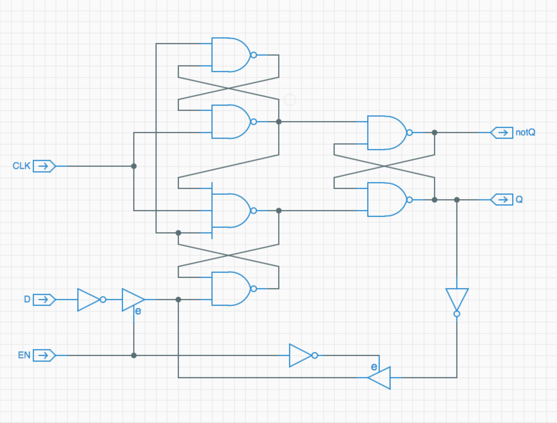
The flip-flops are modified from those described in the "Building Blocks" log entry to include a built-in MUX2, which selects between updating the flip-flop with new data (EN high) or previously stored data (EN low). Note that all of the tri-state buffers are implemented as a single transistor using source as the input, drain as output, and gate as enable. To overcome issues with the body diode in the 2N7000, each signal going into the tri-state must be a isolated from the rest of the circuit. This was done by simply putting an inverter in front of each tri-state input. Yann Guidon pointed out that I could have also used two transistors, rather than a transistor and an inverter. I had explored this earlier, but abandoned it for reasons I can't quite remember (might have had to do with a lower voltage output for that configuration). Since it spares a resistor, I'll likely use it for later additions to the Spikeputor CPU.
Since notQ is the actual desired value of the bit (because D is inverted before the tri-state), an LED was wired directly to that output to show the state of each bit. The two channel outputs actually come from Q, followed by an inverter leading to the tri-state buffers shown in the schematic. Note that for R7, the data values are hard-wired to ground, nor is there any circuitry for writing to or storing in R7, creating the "always zero" register.
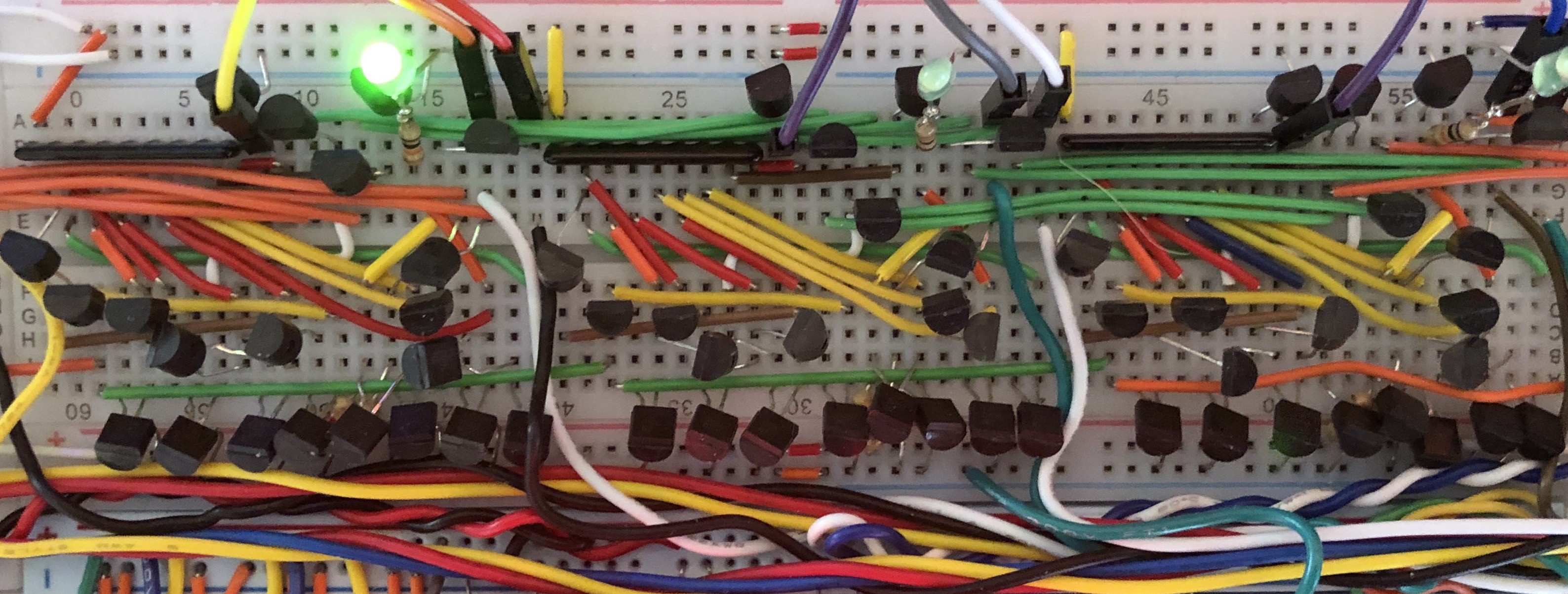
Each register is arranged in a single row on the pegboard, with one breadboard containing the decoder logic and bit 0 of the stored value, and five breadboards with three bits each completing the remaining 15 bits. The decoder also has three LEDs to indicate if the register is selected for writeback (blue), or channel A (red) or B (green) output.
Decoder logic and Bit 0:
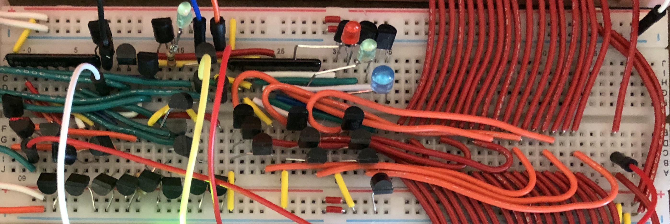
Three bits of Register Memory:
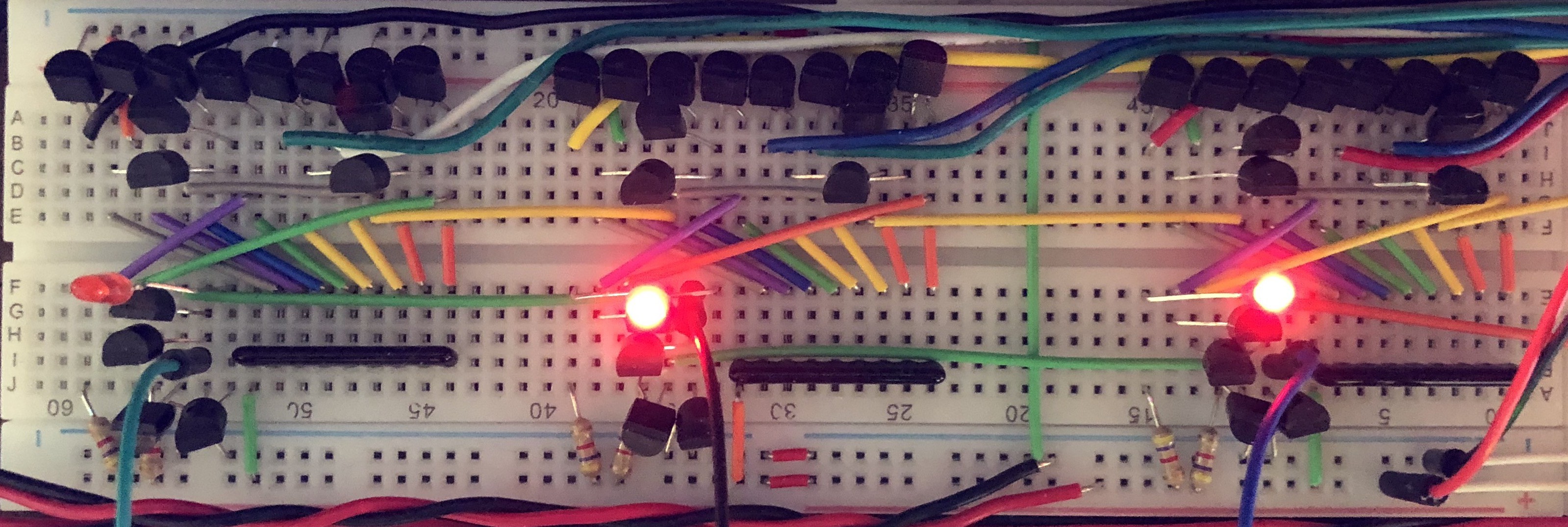
Because I had space, the Writeback Data MUX4 used to select the RegMem WDATA input was placed at the top of the RegMem pegboard. It is also five breadboards wide (three bits per board), plus an additional board for Bit 0 plus the rest of the logic to process the RegMem control signals. The WDSEL signal selects which input (PC_INC, ALU, or MEMORY) is used for WDATA. At the time of the initial design, the fourth input on the MUX4 was open. Since I had the space to accommodate it, I kept it open, initially grounding each bit of the signal, figuring I'd have another way to write a zero to a selected register. As it turns out, as of today, I think I'm going to need this open position to capture the current PC value to handle interrupts, but that's still being worked out. Bottom line: I'm glad I had the inkling to leave it rather than spare some transistors to build a MUX3 instead.
WDATA Input from WDSEL MUX4:
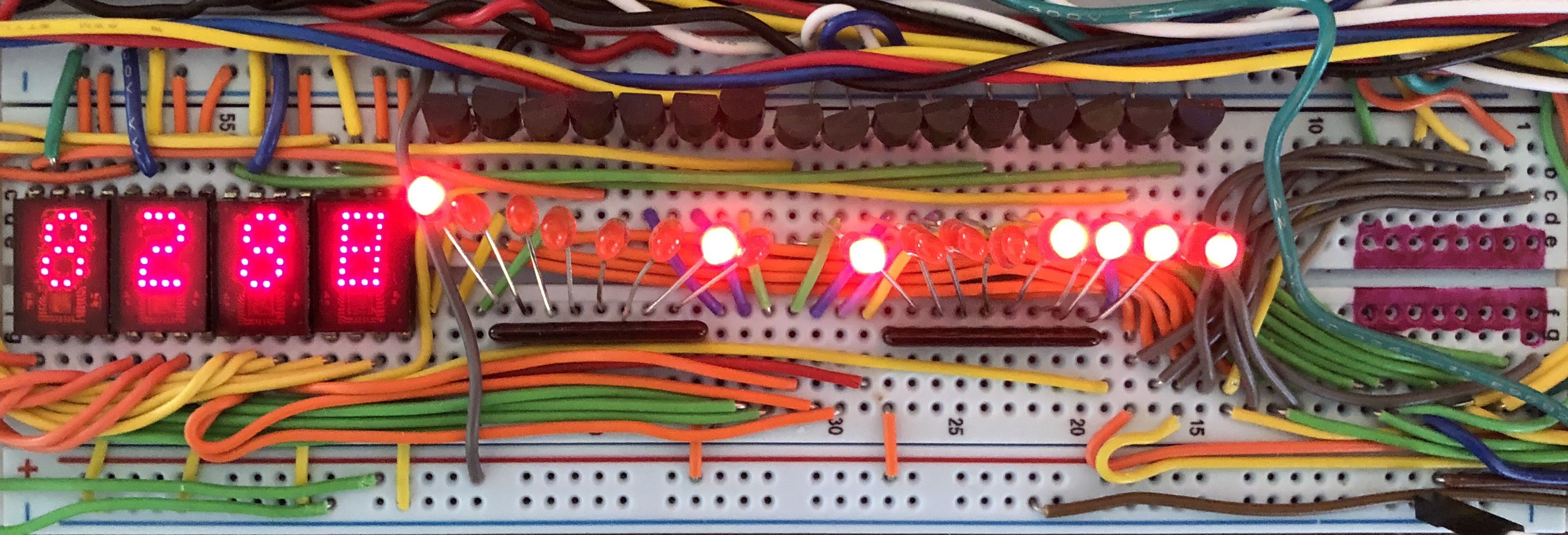
Since register R7 is zero only, it only needed two boards (one for each output channel) to lay out all of the associated tri-state buffers. That left room for two boards to display the RegMem output, both in binary using 16 LEDs, and as a hexadecimal number using HP-5082-7340 display chips (they were way too expensive, but I got them anyway because They. Are. So. Cool.) Note: that last digit appears all-on because when the photo was taken, the associated register was rapidly cycling through all 16 values of the least significant digit. Also note the red-colored area on the board which will serve as the output bus from this channel of RegMem.
Lastly, there was one more open space on the bottom of the pegboard to house the RADATA Zero Detect logic, which is just a big NOR tree:

Here's how things stand as of today. I have completed all 16 bits of registers R0, R1, and R6, four bits each for R2, R3, R4 and R5, and all of the input and output components, including "always zero" R7.

After completing the first two registers and the input and output rows, I started working on the ALU, which will be the subject of the next few logs. As I post those, I'll also be working on finishing the Register Memory. Then, it'll be time to build the control logic that will turn this monstrosity into an actual CPU!
Discussions
Become a Hackaday.io Member
Create an account to leave a comment. Already have an account? Log In.