spudfishScott
-
An Abrupt, if Satisfying, Ending
07/21/2022 at 15:50 • 0 commentsThe Spikeputor, while technically unfinished, has exceeded my initial expectations.
It has performed as a completely functional computer, running at a maximum speed of about 3 kHz, driving text and graphical output, performing relatively complex calculations (Mandelbrot set rendering, digits of pi calculation), and looking great while doing it all!
However, as expected at the outset, the connections within and between the protoboards are getting flakier and flakier. I was spending more and more time wiggling wires and debugging to get the thing up and running, and less time writing Spikeputor code and planning to complete the project with hand-made "display" memory. Rather than spending a lot of time and effort (>3,000 transistors) on that, I've decided to end this prototype project and focus future efforts on a more permanent solution. The Spikeputor Mark ][ will be mostly the same design, with a few modifications to make it even more robust, and rendered on printed circuit boards. I'll post a link to the new project here once I start it up.
In the meantime, thanks so much for following along or taking a peek at what has been an incredibly rewarding project. Spikeputor Mark I out!
![]()
![]()
![]()
-
The Spikeputor Goes Public!
07/25/2021 at 17:07 • 0 commentsI discussed the Spikeputor and its Apple ][ interface at KansasFest 2021 (link), a conference for devoted Apple ][ (and ///) fans. Here's the talk, which I pre-recorded for the virtual event, followed by a live Q&A session:
-
The Spikeputor Celebrates Pi Day
03/14/2021 at 13:54 • 0 commentsIt's been awhile since I've posted an update. I've been mainly doing a bit of re-wiring and re-working to make the Spikeputor more robust. That will all be reported in due course. Meanwhile, It's Pi Day (3-14), so I wrote some big number math routines and had the Spikeputor calculate pi to 80 decimal places using Machin's formula. Enjoy!
-
Input/Output: Keyboard and Displays
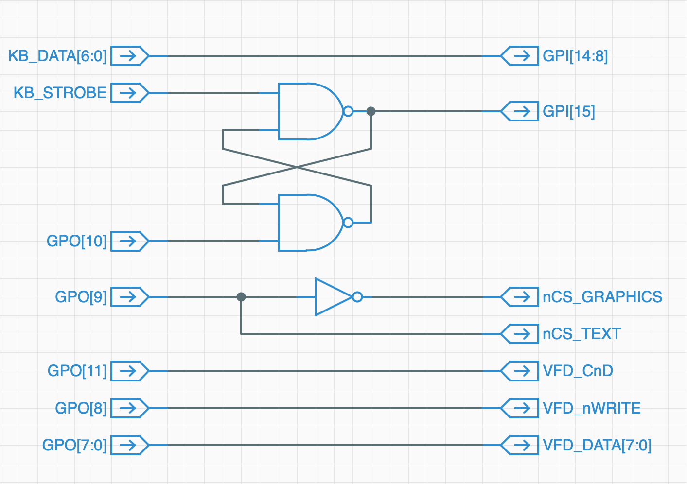
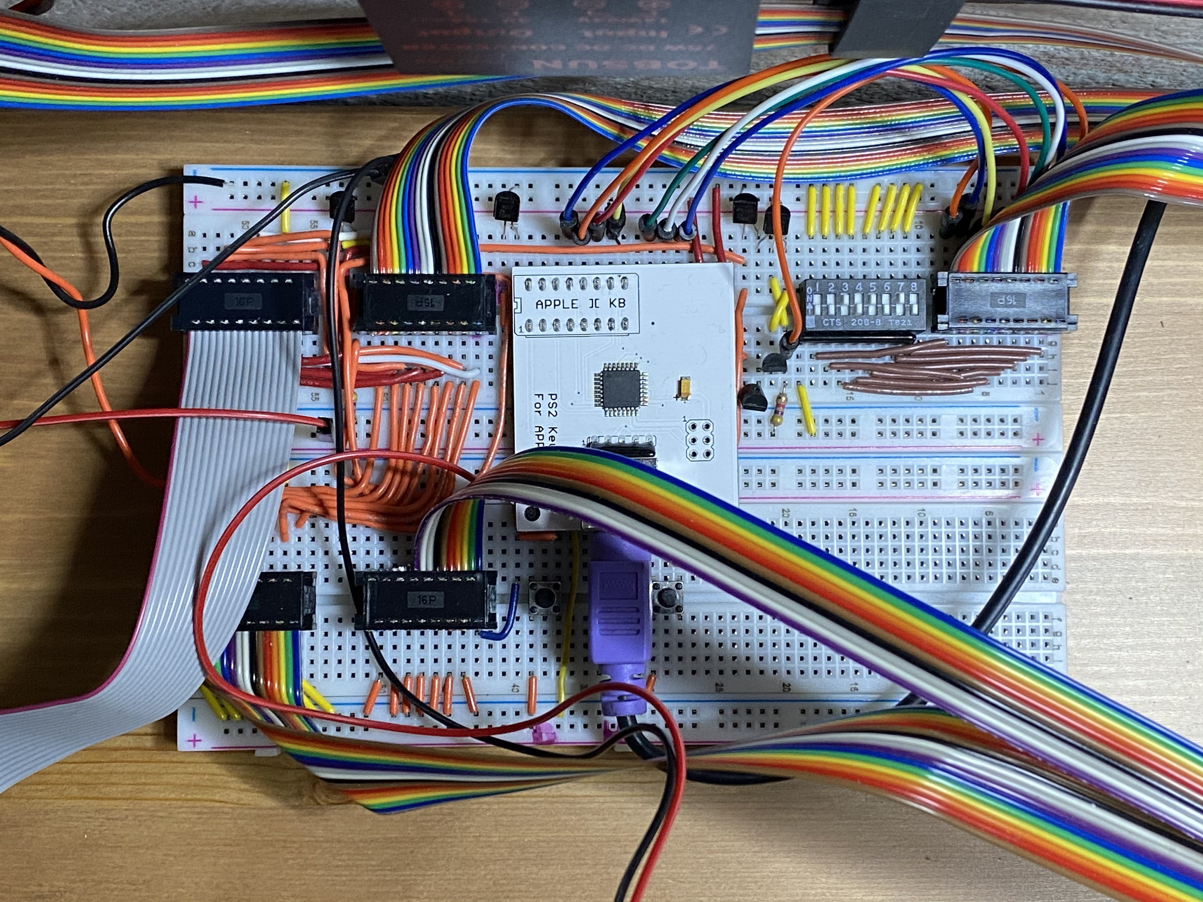
07/20/2020 at 18:00 • 0 commentsUsing the Spikeputor's general purpose input and output feature, it was easy to directly connect a keyboard and two vacuum fluorescent displays, augmenting the BIAS-related I/O described in the previous log entry and providing true stand-alone I/O. Due to the low speeds of the Spikeputor, a parallel approach was taken for both input and output devices. There aren't many parallel keyboards available, but there are several keyboard adapters that will convert standard PS2 or USB keyboards to a parallel signal, mainly for retroputing use. Thus, a PS2 keyboard adapter for the Apple ][ (see this link) was hooked directly to the Spikeputor's general purpose input (GPI) bits 15 through 8. A small amount of hardware logic was added so the Spikeputor could track when a new key is pressed, taking advantage of the same hardware system that the Apple ][ used. The high bit of the GPI is connected to the output of an S-R flip-flop. The SET input of the flip-flop is connected to the STROBE output of the keyboard, and the RESET input is connected to a single bit (bit 10, in this case)of the Spikeputor's general purpose output. To read the keybaord, first reset the flip-flop by clearing and resetting bit 10 of the memory address mapped to the GPO. Then, read the top eight bits of the GPI until the STROBE bit goes high (a key has been pressed). Clear the strobe as before to get ready to read the next keypress and report the ascii value of the keypress. The Spikeputor code for reading from the keyboard is shown here. Recall from the Memory discussion that GPO and GPI are special memory locations $7FFC and $7FFE, respectively, and STRB_MASK is 0b0000010000000000.
![]()
Two Noritake VFDs were used as displays. One is a 2 x 40 character display which accepts ascii input for characters and commands. The other is a 128 x 64 pixel display. Both have parallel interfaces for quick data transfer, eliminating the need for excess computation on the Spikeputor side. Each display works by clearing a ~CS input, setting the data bits of the parallel interface, and then pulsing a ~WRITE input to latch in the new information. In the case of the graphics display, there is also a C/~D (Command/~Data) input signal, which needs to be set depending on whether the input is pixel data or a command to change the position or set other display parameters. All of these signals derive directly from the Spikeputor GPO as shown in the following schematic (which also includes the keyboard input logic):
![]()
Note that bit 9 of the GPO serves as a Text/Graphics output switch so they can share all of the other signals coming from the Spikeputor.
The actual I/O board is shown below. The general purpose input line is in the upper right. the DIP switches set bits 0-7 of ther Spiekputor and are reserved for future inputs. The PS2 to Apple ][ Parallel adapter is in the center, just to the left of the flip-flop circuitry (four transistors). The General Purpose Output line from the Spikeputor is immediately to the left of that on the top. The two cables on the bottom go to the graphics display and the gray cable on the upper left goes to the text display.
![]()
Here's a demo of both text and graphics output and keyboard input. The demo is running at full speed (3.3 kHz), showing that even simple graphics commands such as line drawing are currently quite slow, but definitely workable!
The Spikeputor is now a full-function computer! Further refinements will be a load/save capability through the BIAS/Apple ][ system, a ROM image, including important BIOS routines as well as a functional monitor, a pegboard of hand-made memory, and some additional inputs and outputs.
-
Input/Output: The BIAS System
07/09/2020 at 14:04 • 0 commentsNow that the CPU is complete, it was time to design methods for the Spikeputor to communicate with the outside world. First up, taking advantage of the DMA interface described in the Memory log entry and using it to upload programs to the Spikeputor and to establish two-way communication protocols. As mentioned in the project description, an old Apple ][ Plus was chosen as the primary I/O device for extra retroputing flair. To implement this functionality, two PCBs were designed and fabricated. First, a generic SPI Controller card was made to plug into an Apple ][ peripheral slot. That project is described here: SPI Controller Card for the Apple ][.
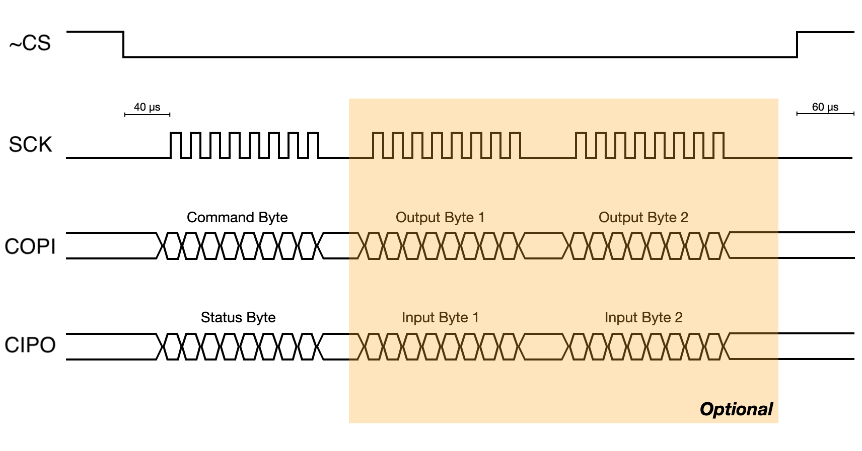
To convert raw SPI commands to operations that can halt, reset or interrupt the Spikeputor, transfer data to and from the Spikeputor, and poll important Spikeputor signals (CLK and ISEL), an SPI peripheral board was designed. The board has five connectors. One connector goes to an SPI Controller card with the standard SPI signals (~CS, SCK, COPI, CIPO). The other four connect to 1. the Spikeputor control signals (comprised of four outputs: ~IOFLAG, IO_WE, RESET, and IRQ, and two inputs: CLK and ISEL), 2. the Spikeputor address bus, 3. the Spikeputor data out bus, and 4. the Spikeputor data in bus. Address and data connectors are 16 bits wide, so the Spikeputor DMA module can be controlled directly by this card. The card can respond to one-byte commands or three-byte commands as described below. Each command transaction starts when the SPI channel is set low and is completed when the SPI channel is set high. To allow for the slow Spikeputor address and data buses to stabilize, wait at least 40 µs after starting the SPI transaction before sending and receiving bytes, and wait at least 60 µs after the end of the SPI transaction before starting a new transaction. Bits are latched into the card's shift registers on the rising edge of the SCK pulse. Clock speed is set from the Controller card of the Apple ][ and this board works well with the on-board clock signal (2 MHz).
![]()
The board responds to eight commands. The command is in the high nybble of the first byte sent. The low nybble is ignored. Three bytes are buffered on the card, so for single byte commands, two extra bytes and be sent and received with no ill effects. Commands are executed at the end of the SPI transaction (when ~CS is asserted). The command set is as follows:
- Command 0xF0: HALT (one-byte command) - Waits until the Spikeputor ISEL signal is high (beginning of CPU Phase 0) and clears the ~IOFLAG signal, which halts the Spikeputor and sets the Address and Data Out selectors to the BIAS lines.
- Command 0xE0: RESTART (one-byte command) - Restarts the Spikeputor immediately by asserting the ~IOFLAG signal. This restarts the Spikeputor clock where it was stopped, at the beginning of CPU Phase 0, and returns control of the data and address busses to the Spikeputor CPU.
- Command 0xD0: IRQ (one-byte command) - Waits until the Spikeputor ISEL signal is high (beginning of CPU Phase 0) and asserts the Spikeputor IRQ signal until the ISEL signal transitions from low to high again. The is required for the Spikeputor to successfully execute an interrupt request.
- Command 0xC0: RESET (one-byte command) - Waits until the Spikeputor CLK signal is high and asserts the Spikeputor RESET signal until the next clock pulse, insuring the completion of the Spikeputor RESET cycle regardless of Spikeputor clock speed.
- Command 0xB0: AUTO INCREMENT (one-byte command) - After this command is executed, the current Spikeputor Address Bus will be auto-incremented after each subsequent READ or WRITE command. Useful for sending multiple words to or from the Spikeputor.
- Command 0xA0: SET ADDRESS (three-byte command) - After this command is executed, the current Spikeputor Address Bus will be set to the value of the word specified by Output Bytes 1 and 2 (big-endian) starting with the next command. AUTO INCREMENT is disabled after this command. The address bus stays the same unless a new SET ADDRESS command is issued or AUTO INCREMENT is re-enabled.
- Command 0x90: WRITE (three-byte command) - After this command is executed, the value of the word specified by Output Bytes 1 and 2 (big-endian) is written to the current Spikeputor address bus location. If AUTO INCREMENT is set, that address is incremented before the write takes place.
- Command 0x80: READ (one-byte write, three-byte read command) - This is a dummy command that does nothing but set the Spikeputor Address Bus to the next value (if AUTO INCREMENT is enabled). Since the Input Bytes 1 and 2 always reflect the status of the Spikeputor Memory Data Output bus, they can be read to get the value of memory at the current address.
The status byte emitted during each SPI transaction can be interpreted as follows:
- Bit 7 - Current value of ~IOFLAG output
- Bit 6 - Current value of IRQ output
- Bit 5 - Current value of RESET output
- Bit 4 - Set if AUTO INCREMENT mode is active
- Bit 3 - Current value of Spikeputor ISEL signal
- Bit 2 - Current value of Spikeputor CLK signal
- Bit 1 - Bit 2 of current Address Bus output
- Bit 0 - Bit 1 of current Address Bus output
The Input Bytes 1 and 2 emitted during each SPI transaction always reflect the current state of the Spikeputor Memory Data Output.
All output signals can be read at any time through the READ command, even if the Spikeputor is not halted. This might be useful to debug signals and current memory data. IRQ and RESET commands also work, but WRITE and SET ADDRESS commands will not work unless the Spikeputor has previously been halted as that is the only way to transfer control of the Address and Data buses to the BIAS card.
The full schematic and KiCAD project files are in the Files section.
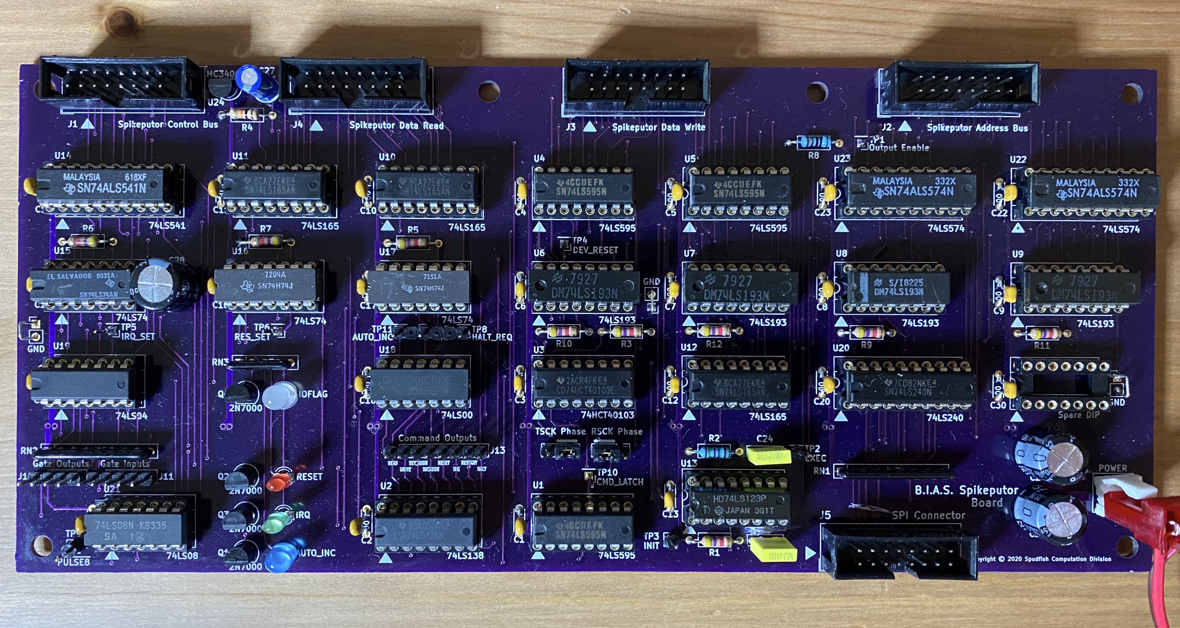
Here's a picture of the completed peripheral board:
![]()
Once the BIAS hardware was complete, a program was written on the Apple ][ to upload machine code to the Spikeputor and execute it. A shared input and output buffer mechanism was implemented in software using Spikeputor memory that can be monitored by the Apple using the BIAS hardware. By using this shared buffer system, the Apple ][ can be used as a simple teletype. By defining some control character sequences to send graphics commands, the Spikeputor can ask the Apple to display text or hi-res or lo-res graphics lines and points. This video shows a demonstration of basic input and output text by displaying prompt strings, accepting input, and reacting to that input with more text and graphics. Although the Apple is handling all Input/Output, the Spikeputor is completely running the show. On the Spikeputor side, this involved writing a suite of low level commands to do multiplication and division, random number generation, string handling, and sending and receiving text output and input through the shared buffers. These routines will eventually be incorporated into the Spikeputor ROM.
-
Installing a Command Interpreter
07/01/2020 at 19:35 • 0 commentsTo determine the current command that the Spikeputor is running, one can look at the INSTRUCTION and CONSTANT registers and work through the bits according to the Spikeputor ISA (described here), but that's a pretty complicated thing to do in one's head and doesn't lend itself to rapid debugging. To promote further understanding of what's going on, we can install a microcontroller-based interpreter which polls the appropriate fetch register and a few key control signals, translates the data into a human-readable assembly language command, and displays the command on a simple alphanumeric display.
All of this was accomplished using an Arduino Duemilanove board and a serial enabled 16x2 LCD display from SparkFun (link here). The inputs were drawn from the 16-bit CONSTANT register. This register is updated with the value of the memory output data bus on each tick of the clock. By including as inputs the CLK signal and the ISEL signal (which goes high at the beginning of each command cycle), the microcontoller can determine when the CONSTANT register is valid for the opcode, and, by examining the opcode, whether or not it would need to look again at the register on the next clock cycle to get the second word of two-word Spikeputor commands.
The microcontroller C code is in the File section (link here).
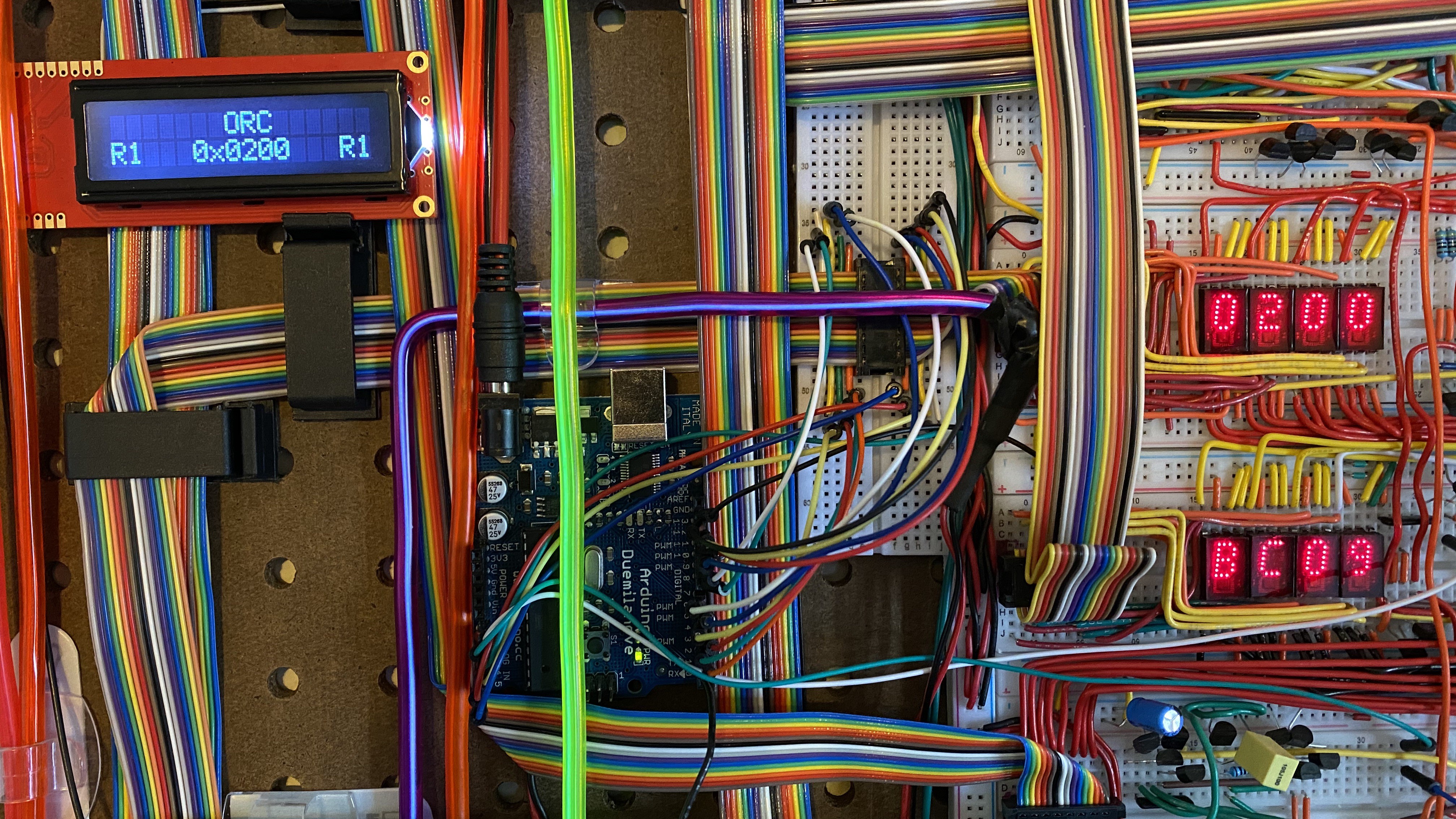
Here's a screen shot of the completed display/microcontroller setup, positioned close to the output of the CONSTANT register.
![]()
At the time this image was taken, the first word of the two word command was first stored in both CONSTANT and INSTRUCTION registers. The microcontroller pulled the value (0xBC09) from CONSTANT, check bit 10, found it was set, and thus waited for the next clock pulse. At that time, the second word of the command (0x0200) was stored in the CONSTANT register (INSTRUCTION is only updated after CPU phase 0). The microcontroller then read this second value, computed the output, and wrote the entire command, ORC(R1, 0x0200, R1), to the display via the microcontroller's serial output.
Here's a video of several Spikeputor commands passing through the interpreter:
-
Electroluminescent Wires Show the Data Paths
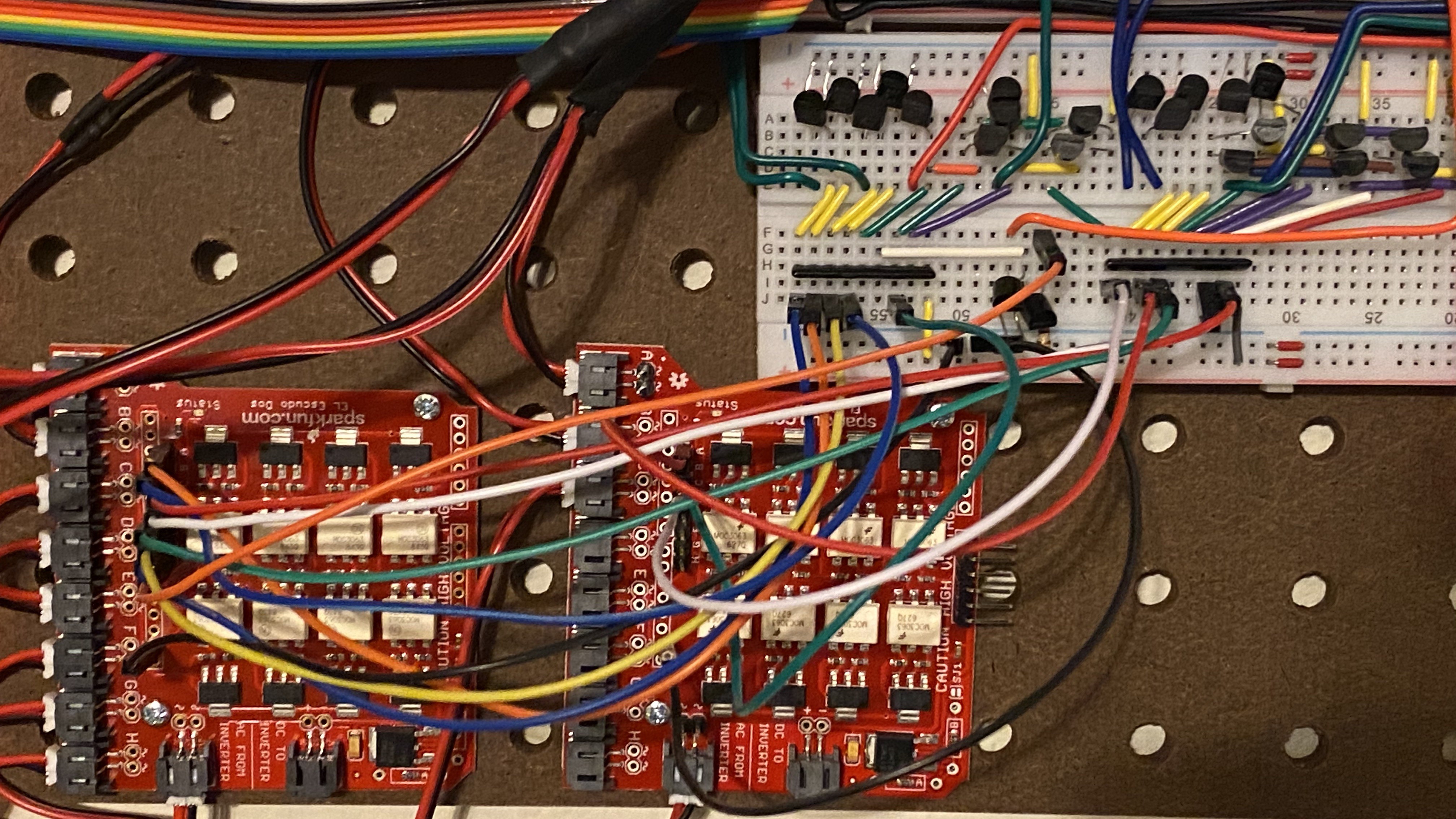
07/01/2020 at 18:32 • 2 commentsNow that the Spikeputor CPU is complete, we turn our attention to the creation of some features to help aid in visualizing the computation, and to creating a fully functional computer via I/O components. While there are LED indicators for all of the important CPU signals, interpreting them at a glance can be challenging. To show the current data paths in a more holistic way, Electroluminescent (EL) Wire was added to the Spikeputor. Each length of wire was placed between two important nodes of the CPU. EL driver logic was added to the third pegboard, and two Sparkrfun EL Escudo Dos boards (see this website for full information, including schematics) were used to convert the logic signals into the high voltage AC required to turn on the wires.
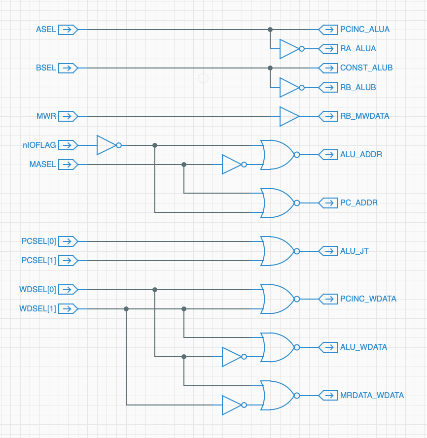
Here's a schematic of the EL Driver logic, showing the Spikeputor control signals as inputs, and the identity of the two connected nodes as outputs. For example, the ASEL signal is used to illuminate EL wire between the ALU Channel A Input and either the Register Channel A Output or the value of the PC Increment register (labeled in the schematic as RA_ALUA and PCINC_ALUA, respectively).
![]()
The driver logic and Escundo boards are mounted in the lower right corner of the third pegboard:
![]()
This video shows the result. The rate of the EL Wire changes can be adjusted by changing the Spikeputor clock speed, or by putting the Spikeputor CPU into single step mode.
-
Completing the Third Pegboard
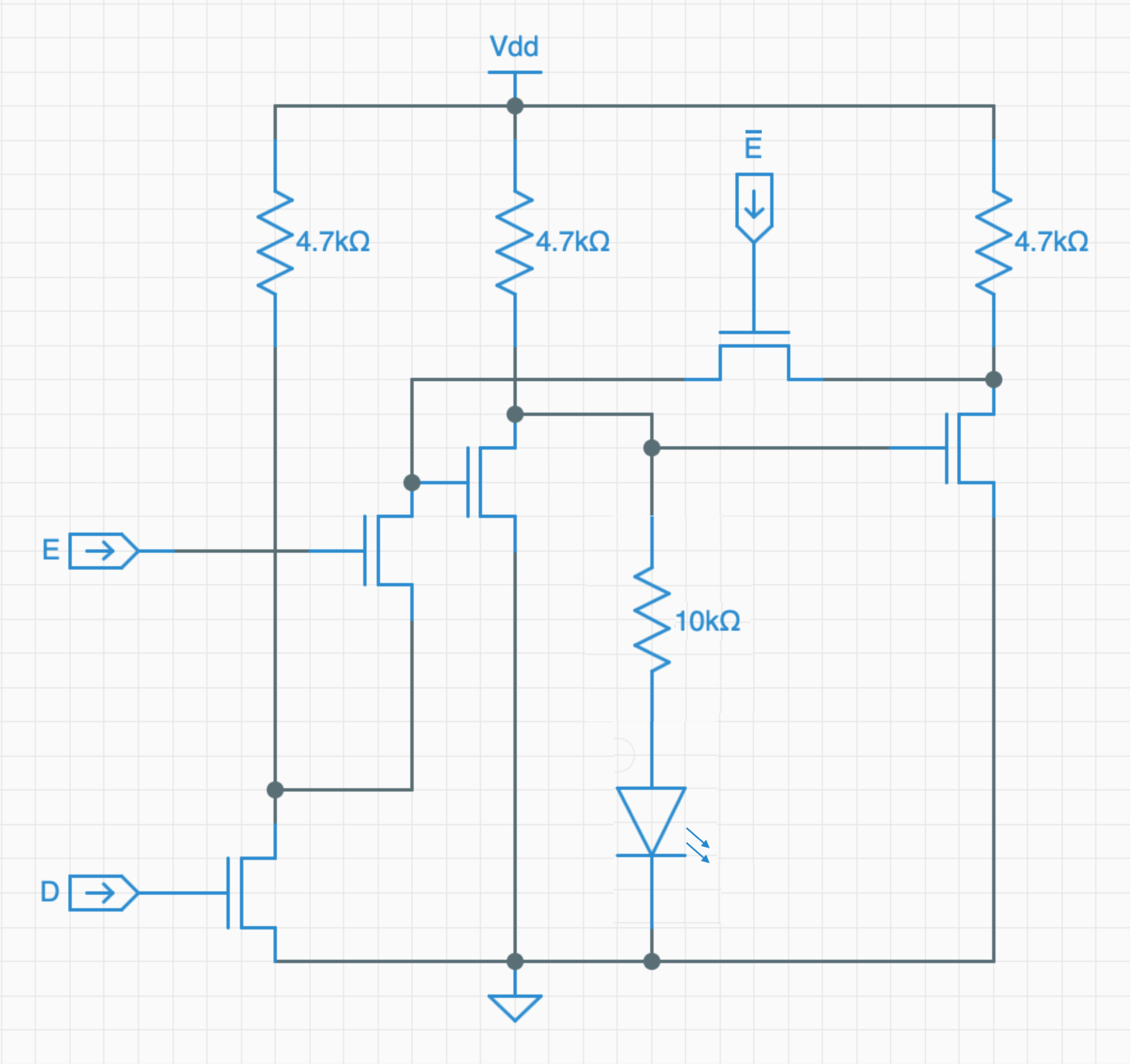
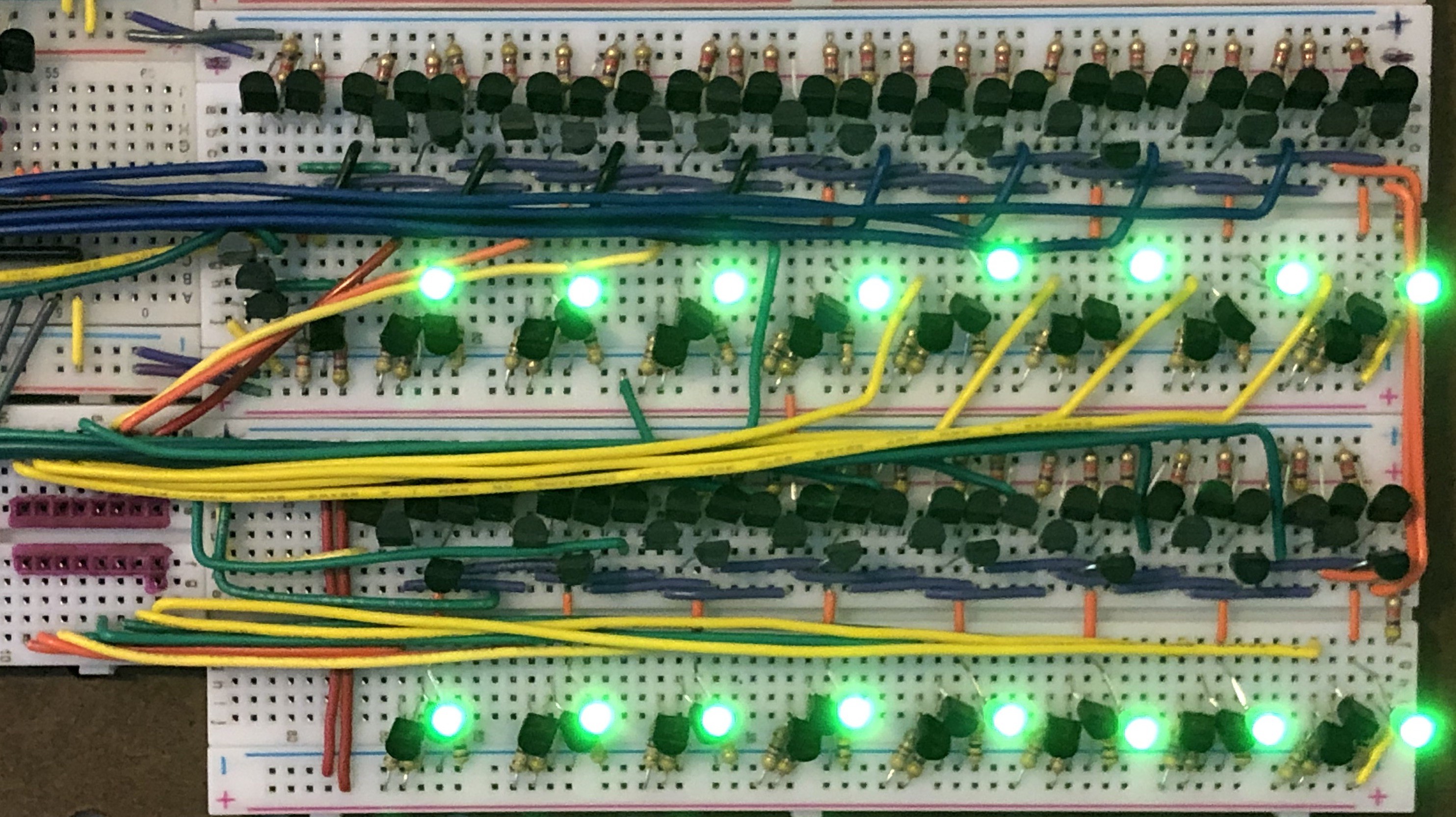
02/29/2020 at 21:48 • 0 commentsThe final two components of the third Spikeputor pegboard, and the last two pieces of the main Spikeputor design, are the electroluminescent (EL) wire driver and sixteen bits of discrete general purpose output memory. The EL wire driver is just a small set of simple logic gates to convert control signals to individual wire output signals – more on that later when all of the EL wire has been mounted. The GPO memory was made based on the design for the discrete static "screen" memory that will be realized on the fourth and final pegboard. The memory design features five transistors, four resistors, and an LED per bit:
![]()
The memory bit is set or cleared by placing the desired value on D, asserting E, and clearing ~E. While the screen memory design is "write-only", the value of the bit can be accessed by buffering the signal off the drain of the transistor on the far right. This is how the general purpose output lines are implemented:
![]()
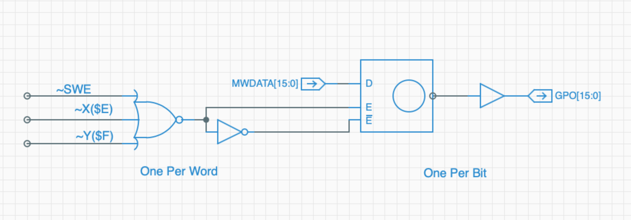
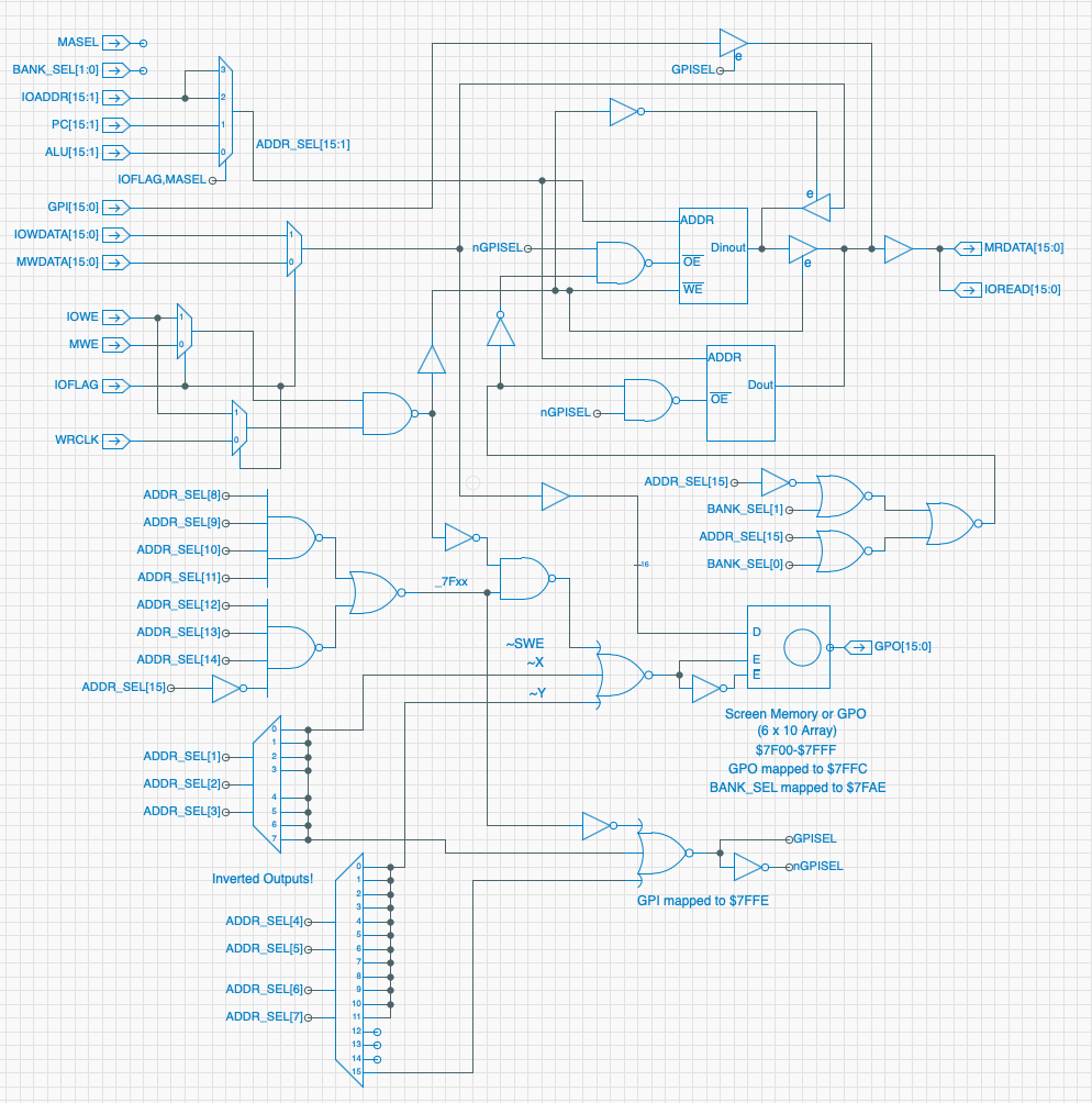
The data lines are pulled directly from the Spikeputor MWDATA bus. E and ~E are set by NORing the appropriate active-low decoded address lines. Writing to any address $7Fxx sets ~SWE low, while the low byte of the address is decoded into twelve Y signals for the high nybbles ($0-9, plus $A and $F) and eight X signals for the low nybbles (only even numbers). So, to write to the GPO, simply store the desired value in memory location $7FFE. Putting it all together, it looks like this:
![]()
The red outline on the lower left indicates where a 16-pin DIP cable can be plugged in to access the output signals. The LEDs reflect the values of each bit. Here's a video that shows a program running that cycles values through the GPO address:
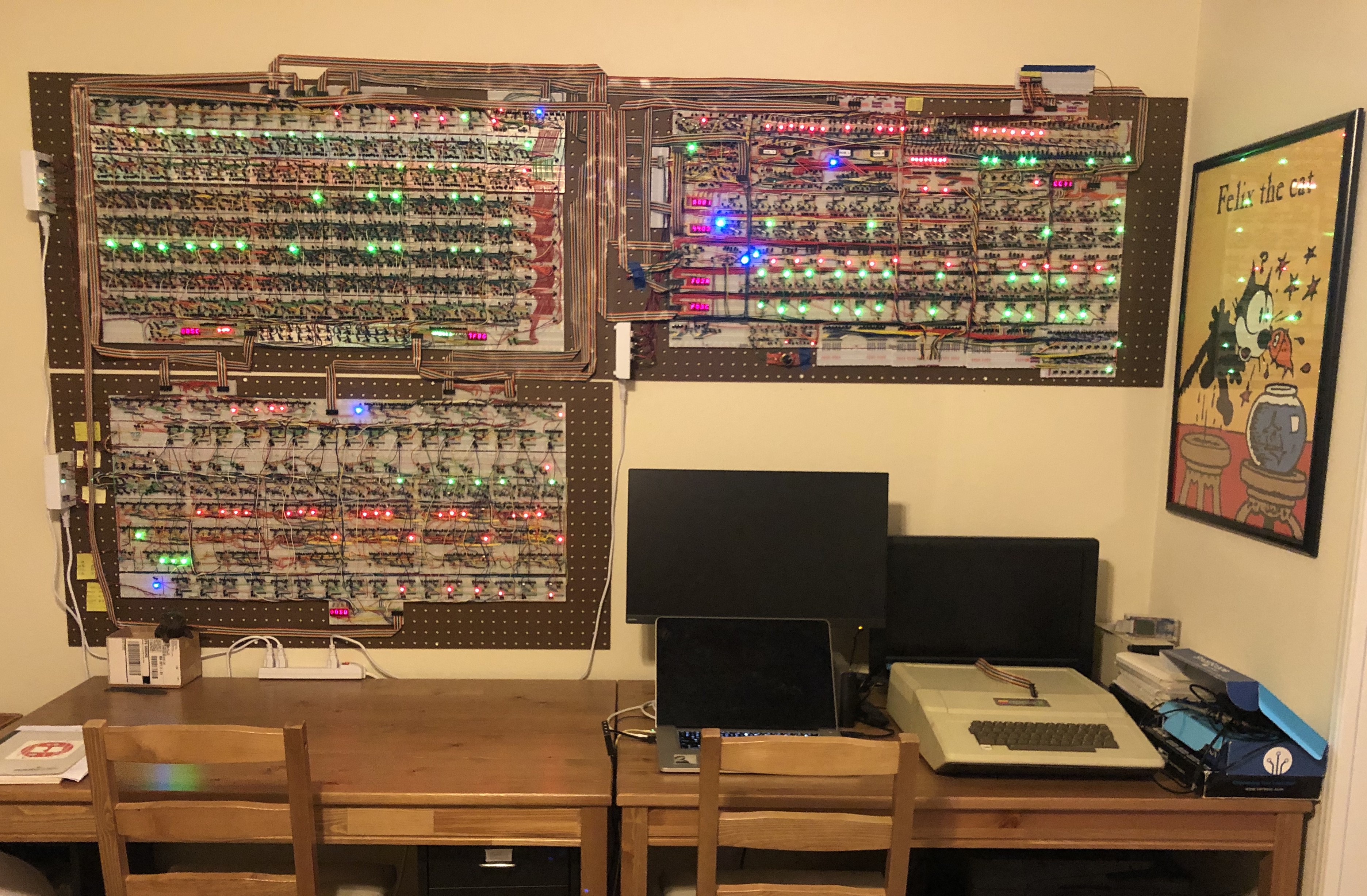
Now that the third pegboard has been completed, it was mounted on the wall, and the cables running between the Spikeputor modules was cleaned up mounted clips. Here's the big picture:
![]()
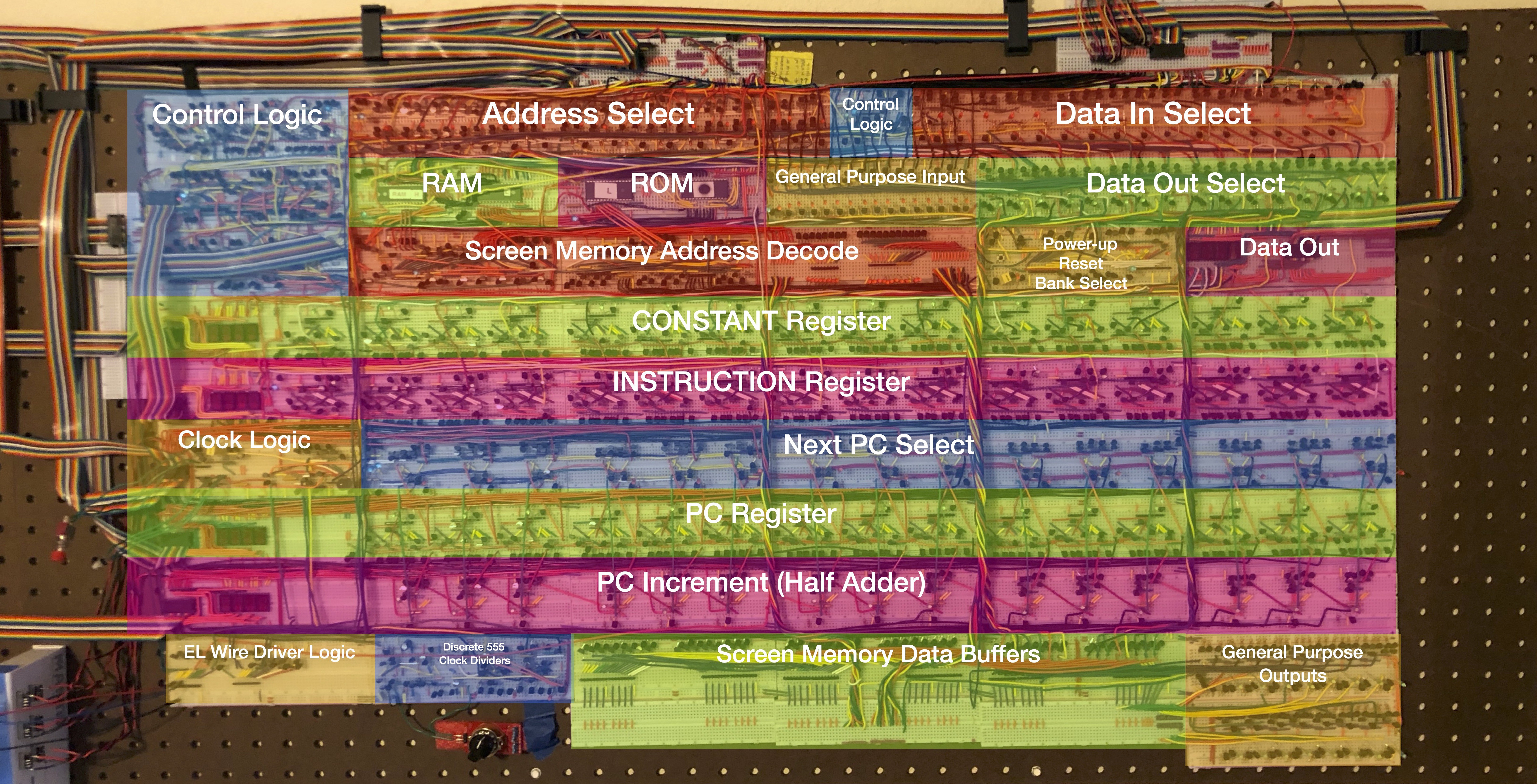
Here's a close-up of the third pegboard with a summary of all of the modules it contains. The previous two pegboards are documented in the sections on the ALU and Register Memory.
![]()
-
Timing Refinements and a Discrete 555
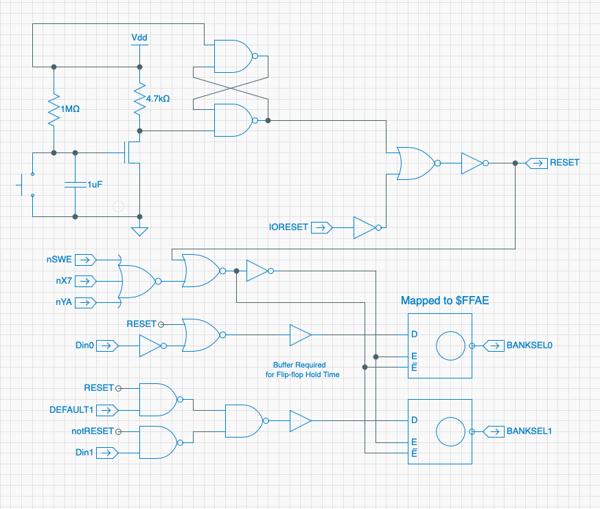
02/03/2020 at 22:40 • 0 commentsNow that the Spikeputor CPU is up and running, it was time to make some refinements. First up, something that I had been toying with for awhile: replacing the 555s used to generate the clock signal (bistable) and to generate a long RESET signal (monostable). I replaced the monostable 555 circuit with a simple RC circuit. This was incorporated into the start-up schematic that was shown in a previous log. The new version looks like this:
![]()
While replacing the bistable 555 circuit for clock signal generation, I reviewed how the Spikeputor writes to memory, as I had been seeing a few glitches in that department. The original design was to trigger the Write Enable signal on the memory chips during the second half of the clock cycle by simply ANDing the inverted clock with the Spikeputor Memory Write Enable (MWE) signal. There were several problems with this approach. First, it gave the Spikeputor only a half a clock cycle to compute the address to write to, effectively limiting the maximum clock cycle frequency. Second, and a bit more concerning, was the fact that there was a possibility that the Write Enable signal might persist while the address bus was changing on the rising edge of the next clock pulse. This could data to get inadvertently written to the wrong location. To avoid cutting it close like that, and to give the Spikeputor more time to compute the address to write to, the following timing was envisioned:
![]()
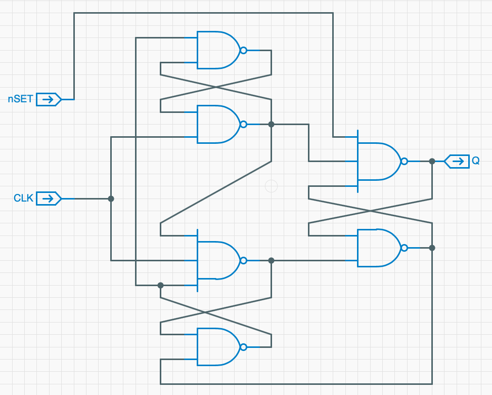
Instead of the Write pulse starting halfway through the clock cycle and ending at the very end, I wanted a pulse that started later and ended before the end of the clock cycle. One relatively easy way to achieve this would be to divide the clock by four and use simple logic gates to generate the desired pulse that starts 3/4 of the way through the cycle and ends 7/8 of the way through. To divide the clock, a discrete Toggle Flip-Flop was designed that toggles its output on every input clock cycle and could also take a SET input, which would be used to reset the new scheme whenever IOFLAG stops the Spikeputor clock:
![]()
The discrete 555 circuit was taken from this great kit: https://shop.evilmadscientist.com/productsmenu/652
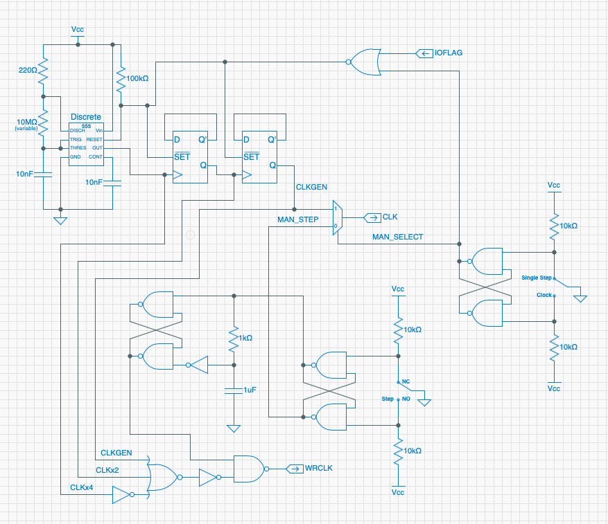
Putting it all together, the new clock schematic is as follows:
![]()
The discrete 555 passes through two T Flip-Flops to divide the signal by 4. The original clock signal and each of the T Flip-Flip outputs are combined via a NOR gate to create the desired proto-signal. This is then OR'd (as created by a NAND with inverted inputs) with a sub-circuit to produce the write pulse a short time after a manual clock pulse, creating the WRCLK signal. That signal in turn replaces the CLK signal input to the memory module, and with a few other small changes to get the phase of the signal right, the new memory schematic is:
![]()
Whew! Here's a video of the new clock generator. You can see the clock signal get divided by two twice.
The discrete 555 circuit is on the left half of the board. Measuring 72mm by 48 mm, it is exactly 64 times larger by area than the classic 555 IC package. Cool!
So now the Spikeputor has a new clock, no more 555 chips, and new write signal timing, allowing me to increase the maximum clock frequency by 25%. Next up, time to finish and mount the third pegboard.
-
And Just Like That, We Have A CPU!
11/18/2019 at 04:45 • 4 comments🚨Phase One of the Spikeputor Project has been completed! 🚨
Integrating all of the modules was just a matter of making cables to connect everything, and writing some Arduino code to load data into the Spikeputor's memory through the DMA model. Here's a video describing the maiden voyage:
Many more things to do, including a bunch of clean-up, making some memory from discrete transistors, adding some more I/O features, and optimizing the top speed.
But for now, I'm just happy the thing actually works!
The Spikeputor
I am building a computer featuring a 16-bit RISC CPU made of discrete transistors for learning, fun and art. It will be pretty large.