Plasmode
-
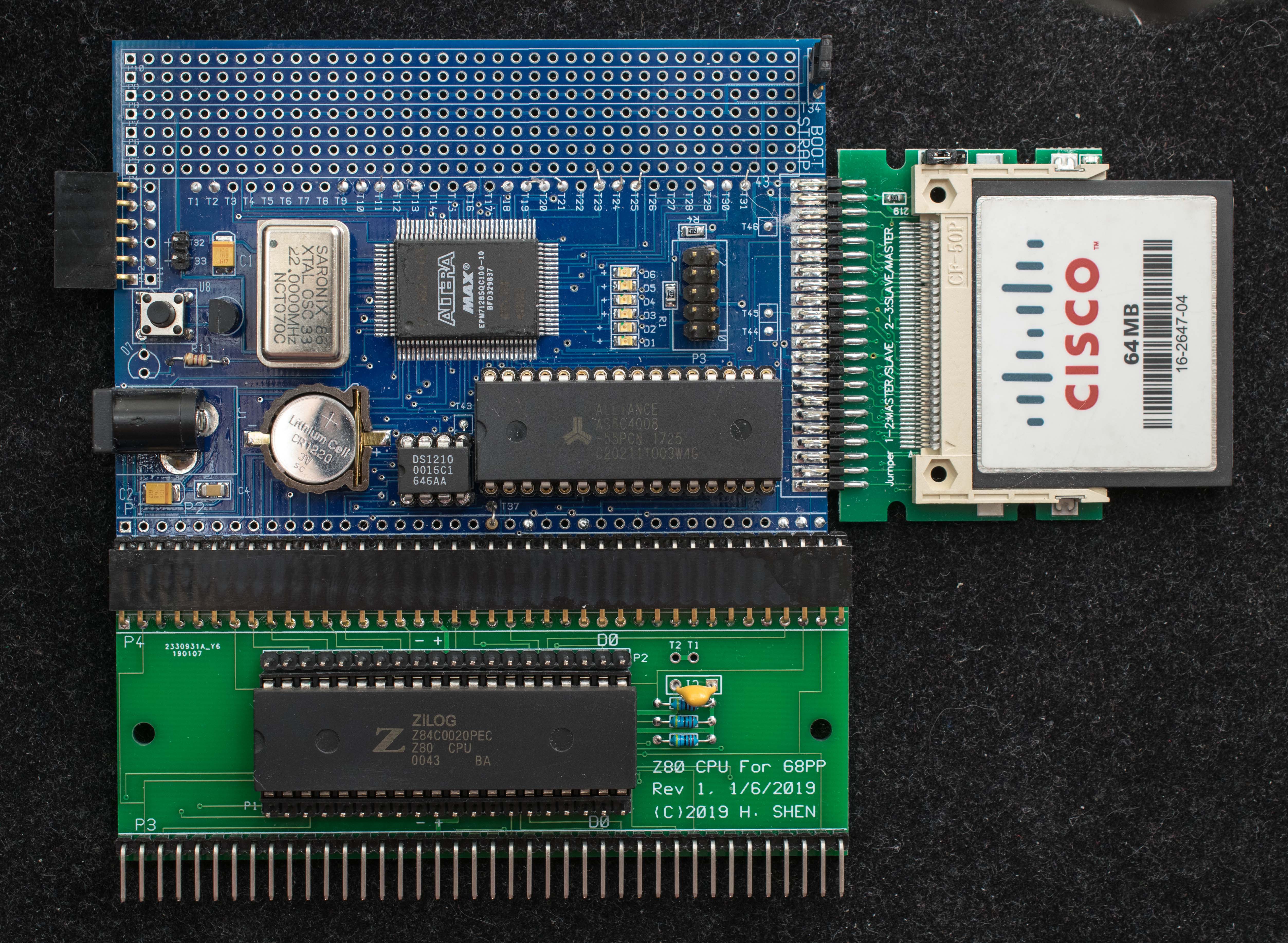
G8PP+Z80, Part 4
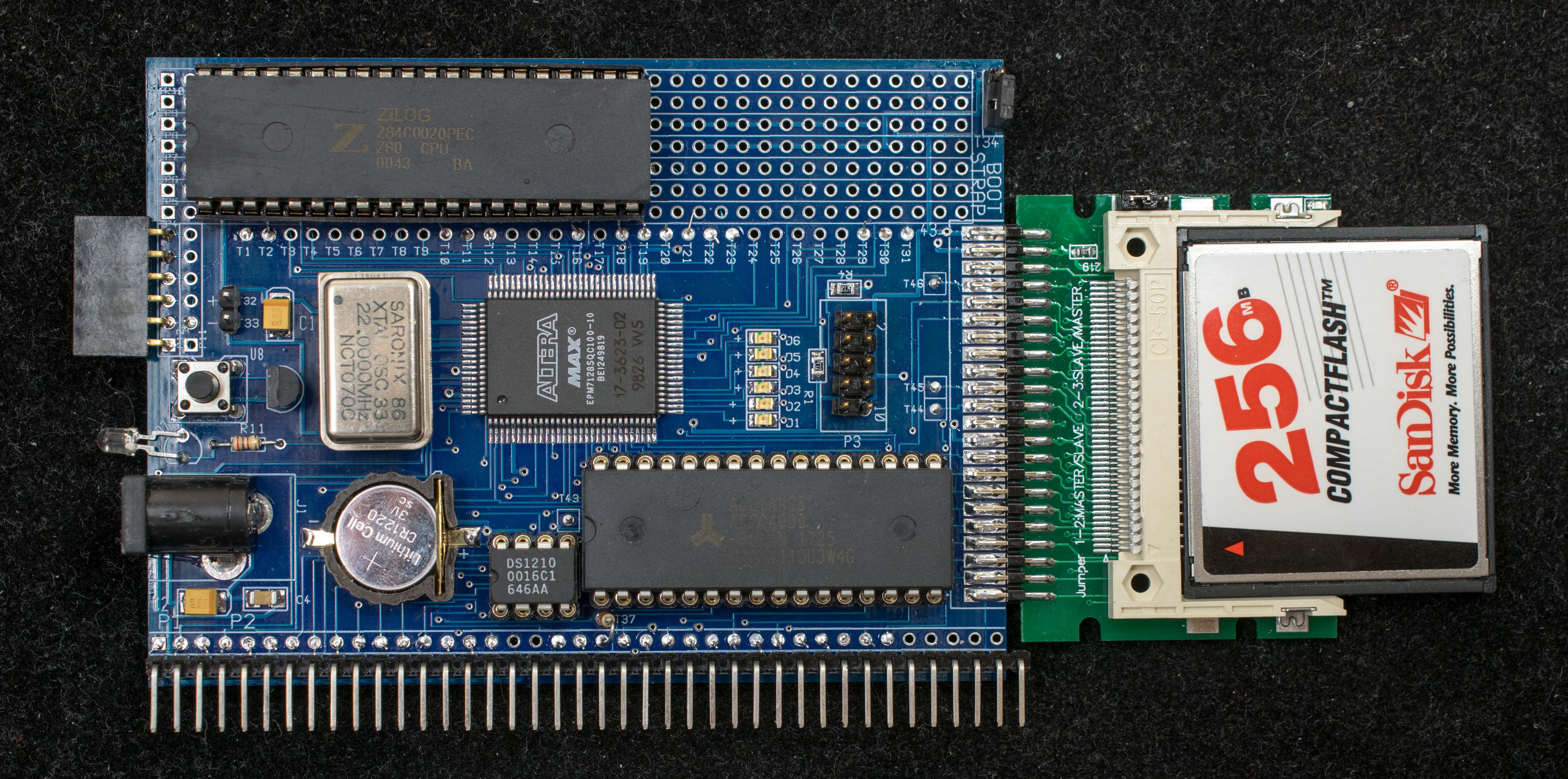
03/01/2019 at 13:38 • 0 commentsI like the idea of two separate boards, a common G8PP memory/IO/CF board, and a CPU board. I've designed 5 CPU boards with that concept in mind. These CPU boards have male RC2014 connector on one side and female RC2014 connector on the other side so the common G8PP board can plug into the female connector resulting in a complete computer without a RC2014 backplane. Below is the picture of such G8PP & Z80 combination. All the software from previous project work on this new configuration.
![]()
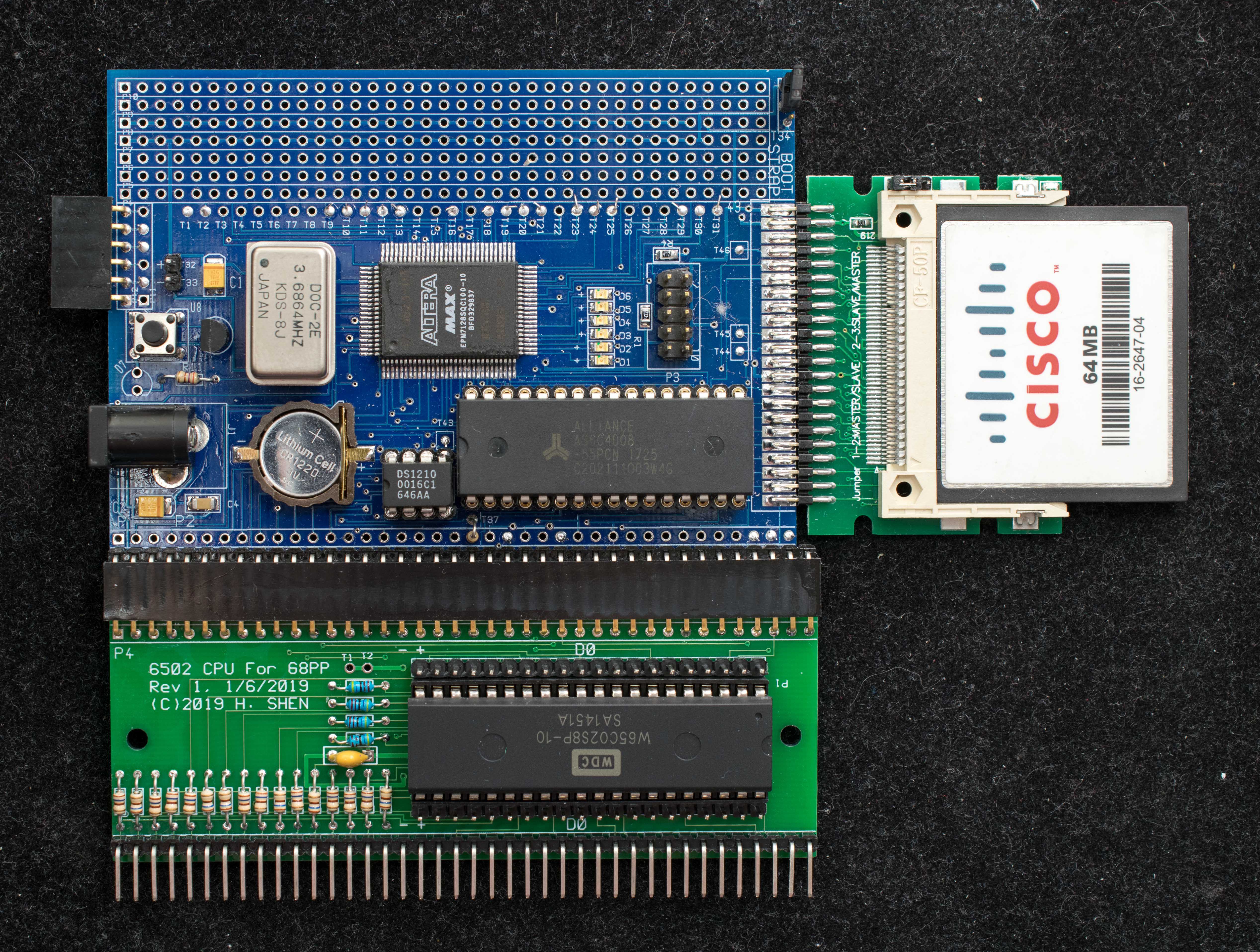
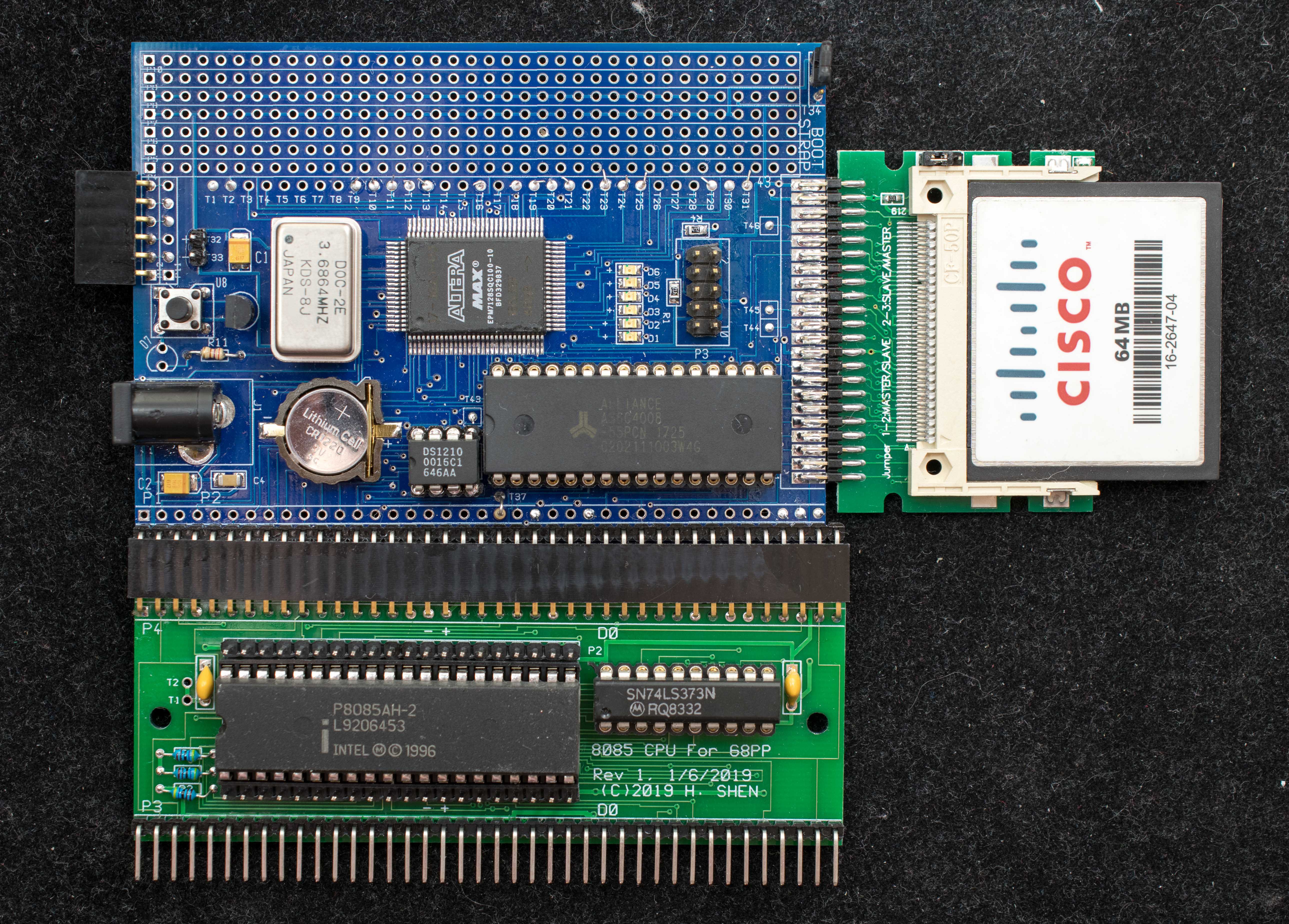
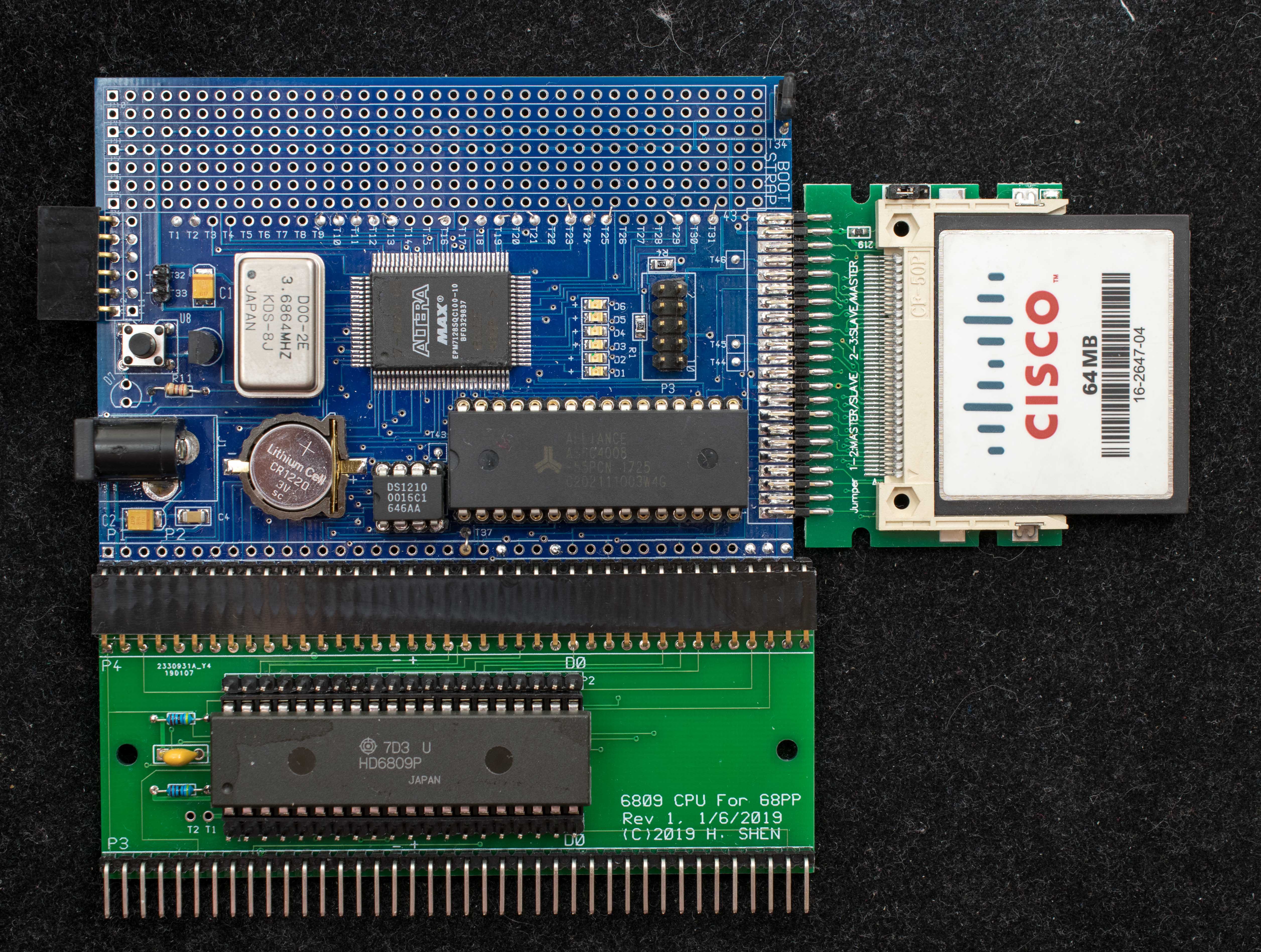
I've spent quite a bit of time on Z80 to develop the G8PP concept. I'll now move more quickly over other 8-bit and 16-bit processors. Below are pictures of G8PP+CPU for 6502, 8085, 68008, and 6809.
![]()
![]()
![]()
![]()
-
G8PP + Z80 Part 3
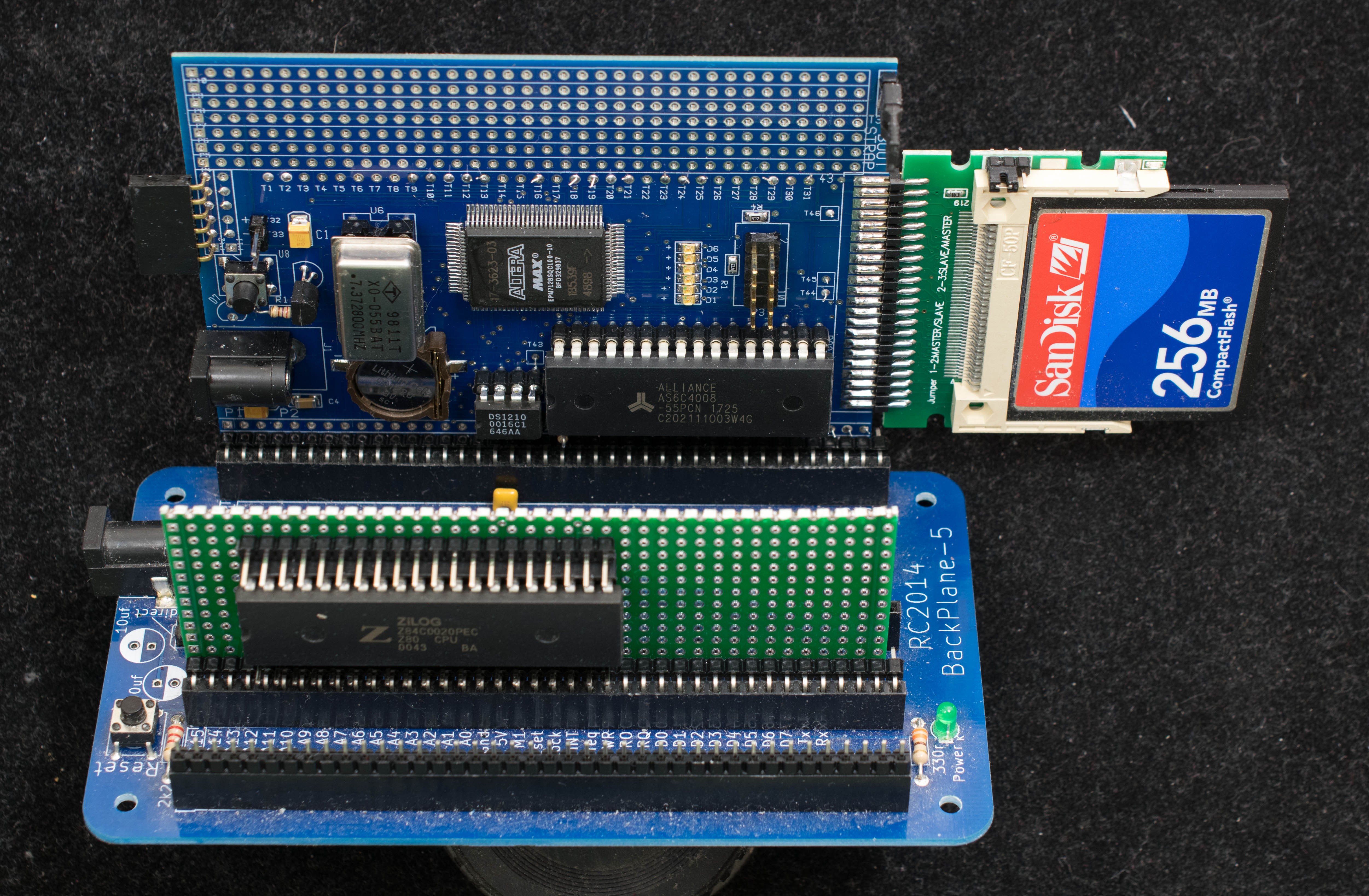
02/06/2019 at 04:47 • 2 commentsG8PP board with processor in its prototype area works well with Z80 and I expect it to work just as well with other 40-pin or 48-pin CPU. However, the prospect of having to manually wire 40+ connections for every processor is unpleasant. A better configuration is having two boards plug into a backplane. Ideally, the G8PP should not be modified physically except the CPLD reprogrammed for different processors. The specific processor is a separate board that plugs into a backplane along with G8PP. The backplane also has additional slots for expansion. The picture below illustrates this concept.
![]()
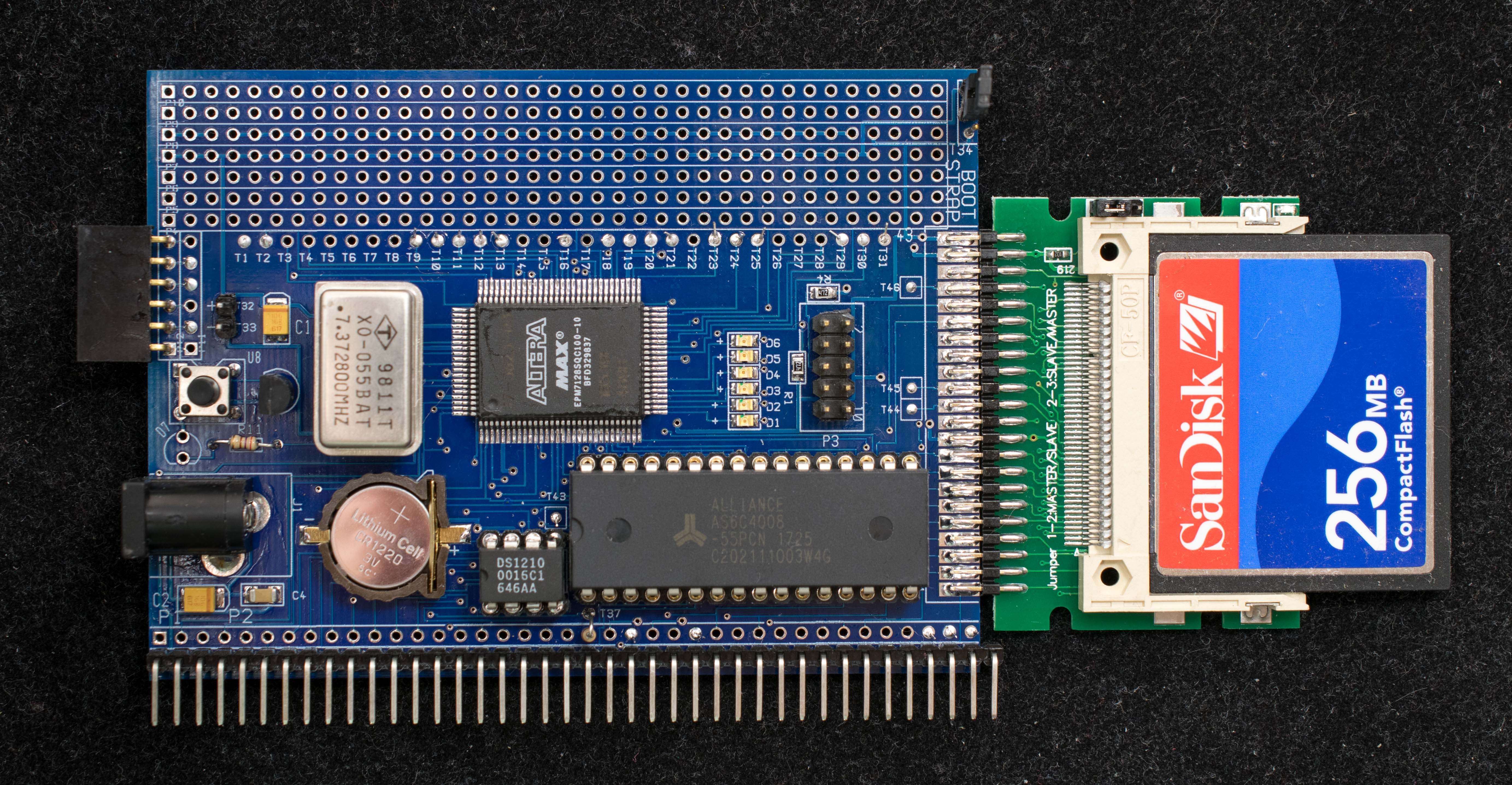
The G8PP+CPU concept is now a two-board system: G8PP in baseline configuration consists of clock, RAM, CF interface, and CPLD. The CPLD can be reprogrammed in-situ to accommodate different processors. No additional manual connections are needed when change processors. The G8PP baseline becomes a pc board without myriad of jumper options. This is the schematic of the G8PP baseline
![]()
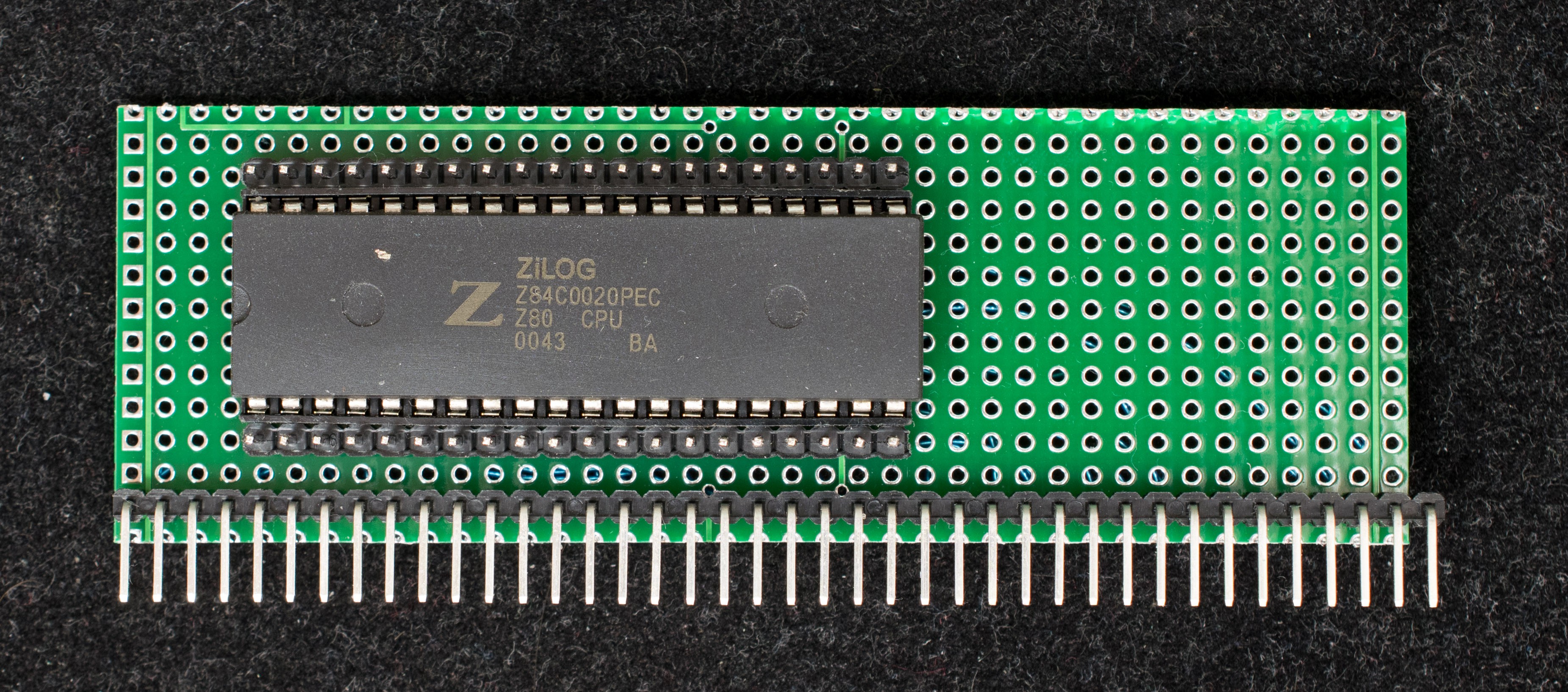
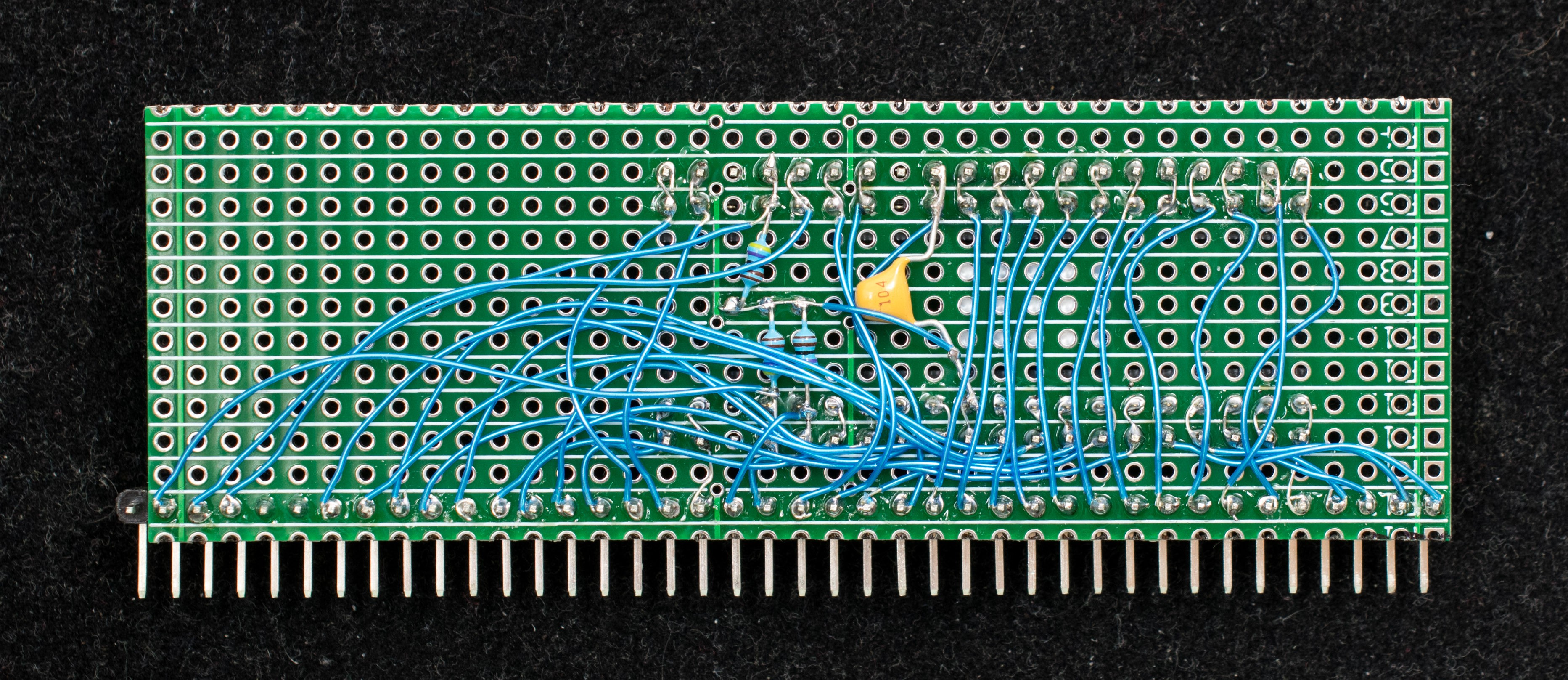
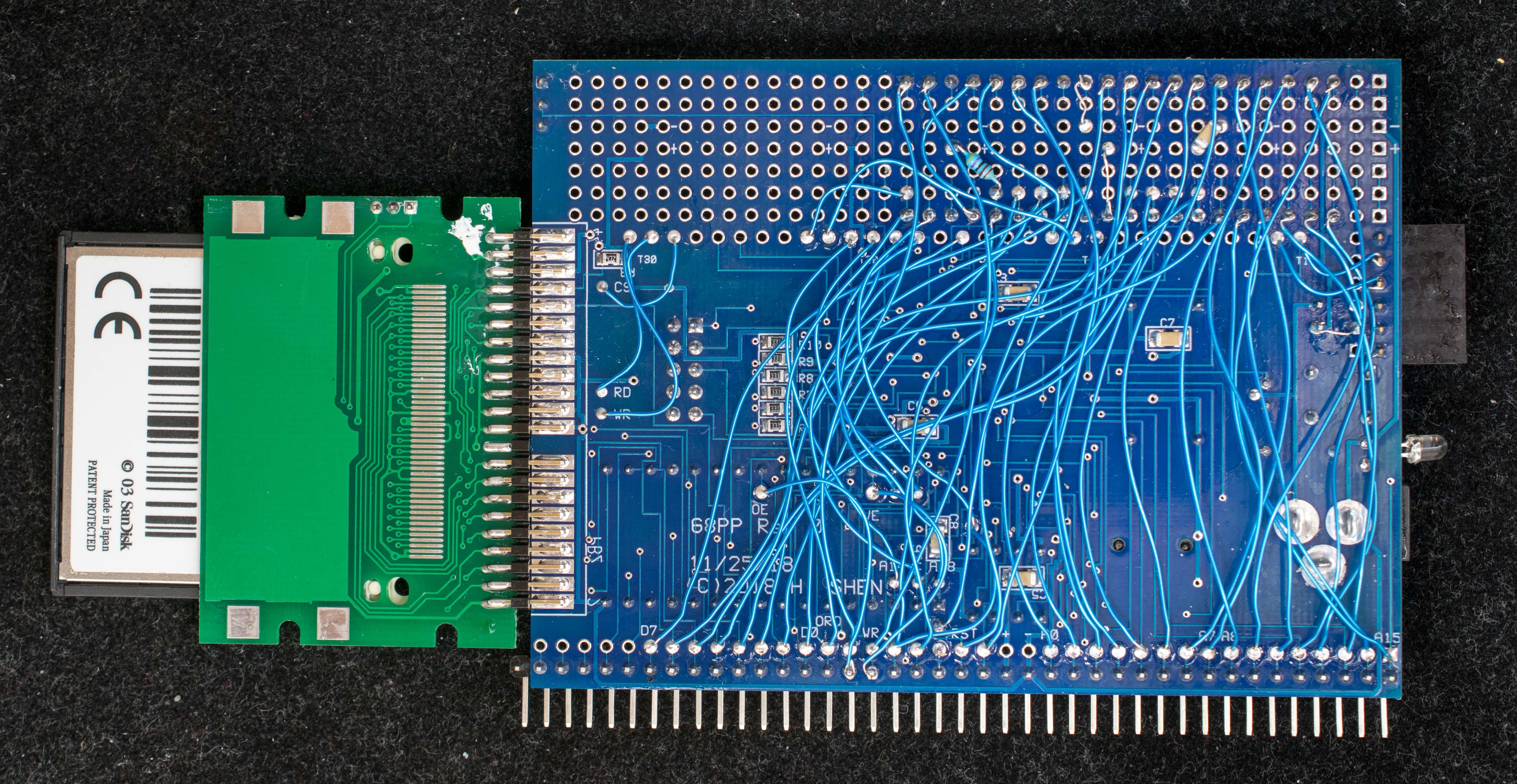
The CPU board is a simple pc board with pre-defined addresses, data, clock, power, and reset pin assignments same as RC2014, and few processor-specific control signals unique to the particular processor. The prototype CPU board in the picture is hand wired, but it can easily converted to a pc board. This is the schematic of the Z80 processor board.
![]()
![]()
The resulting 2-board system work just like the single-board version described in Part 2. All software that run in the single-board version also run in the two-board system.
-
G8PP+Z80 Part 2
02/05/2019 at 05:17 • 0 commentsCP/M is a well known operating system in 1970's and 1980's. It was designed for many different processor family, e.g., Z80, 808x, 68000 and others. Running CP/M is the end goal for many of the processors prototyped with G8PP because that demonstrates the hardware has reached a meaningful level of complexity and functionalities.
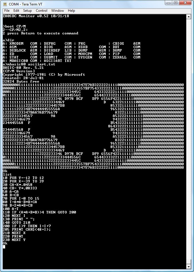
To run CP/M, the computer needs a mass storage, serial port, and RAM memory. This is exactly what G8PP has. CP/M 3 works best with banked memory, the 512K RAM on G8PP can be split into 32 banks of 16K each to support CP/M 3. There are many literature on Internet that describe the process of porting CP/M 2 & 3 to Z80. I won't get into these details here. To support CP/M, additional commands are added to the bootstrap monitor so the CF disk can be formatted and CP/M2.2 CCP/BDOS/BIOS can be installed and retrieved from designated area in CF disk.
This is the steps for installing CP/M into a new CF disk:
- Format the new CF disk using the format command of the bootstrap monitor,
- Install CCP/BDOS/BIOS in designated sectors in CF disk using the copy CP/M command of the bootstrap monitor,
- Load XMODEM.COM into memory starting from 0x100 using the bootstrap monitor,
- Boot into CP/M using the boot CP/M command of the bootstrap monitor,
- It is now in the CP/M environment, type "SAVE 17 XMODEM.COM" to save the memory content as XMODEM.COM. This is the first file created in CP/M directory
- Use XMODEM.COM to bring in the remaining CP/M files. Instead of XMODEM each files individually, I use 'arj.exe' in PC to compress a set of CP/M files and then use 'unarj.com' to decompress them in CP/M.
There are several important tests to run when in CP/M:
- PIP B:=A:*.*[V], which copy with verify the content of drive A to drive B. It is a good CF read/write/verify test to make sure CF disk can read and write without errors.
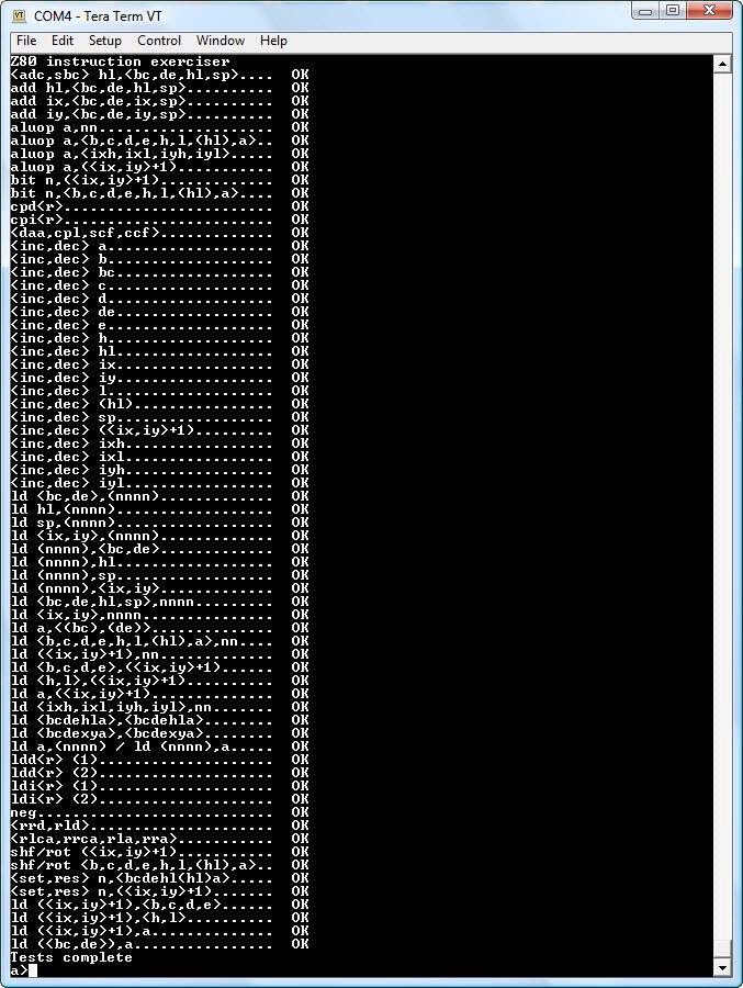
- ZEXALL.COM, this is a thorough Z80 instruction test that takes about 35 minutes to run with 22MHz CPU clock. It should pass 100% thus verify Z80 is functioning correctly at 22MHz.
![]()
- MBASIC80 ASCIIART.TXT to run the ASCII mandelbrot benchmark which should take 52 seconds to run.
![]()
Once CP/M 2.2 is running, it can be used to build CP/M 3 and boot CP/M 3 with 'CPMLDR' command.
The design is quite robust. I'm able to overclock the Z80 to 29.5MHz and verify its functionalities with ZEXALL.COM instruction test. The CF interface is also very stable. I've tested it with 20 different brands and sizes of CF disks and they all worked.
-
G8PP+Z80, Part 1
02/03/2019 at 17:56 • 0 comments![]()
![]()
The original intent of G8PP was to have a prototype area for DIP-40 or DIP-48 processors and enough room for a clock controller which is required for some of the earlier processors such as 8080.
G8PP with Z80 in the prototype area is the logical first experiment. After all, the RC2014 bus which the G8PP is based on is designed for Z80 processor. The first picture shows the Z80 on a G8PP board. The second picture shows the solder side of the board. It is immediately obvious that this approach is a manual-wiring-intensive prototyping. Since Z80 is a 40-pin device, there are at least 40 hand wires. There are additional wiring for banked memory and Z80-specific configurations. Some of the hand wires can be standardized and eliminated in revised G8PP pc board, but CPU's pin-out are not standardized, so 40-pin CPU needs about 40 manual wires that's unavoidable.
Having done the manual wiring, the resulting single-board Z80 is quite capable. Here are its features:
- Z80 clocked at 22MHz
- CP/M 2.2 and CP/M 3 ready
- 512K battery-backed RAM
- 32 memory banks, each bank is 16KB
- Serial bootstrap capability
- Simple serial port, 115200-N-8-1, no handshake
- RC2014 bus compatible
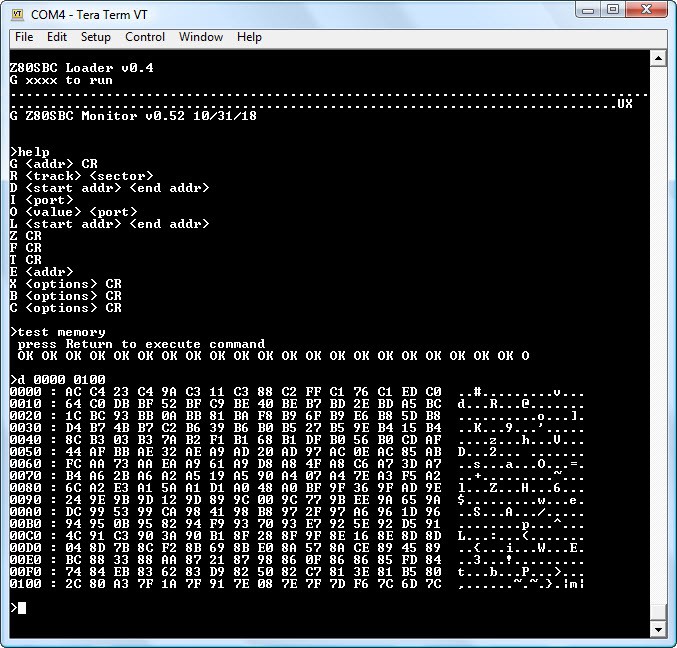
The serial bootstrap code is 255 bytes long and is basically a Intel Hex file loader. Once the code is loaded, the console outputs the sign-on message and waits for more files to be loaded. At the end of file loads, a 'Gxxxx" command executes the program at specified location. Because the RAM is battery-backed and the bootstrap code can be hidden away in one of the banked memory, the serial bootstrap operation only need to be done once. Below is an interactive session showing the process of loading bootstrap and loading a monitor/debugger. Once Z80 boots up and is in control, more files can be loaded; the compact flash interface can store data and files; and more functions can be added through RC2014 expansion bus. This is in fact a compact, high performance Z80 SBC. There are not many Z80 that's this compact and runs at 22MHz. A side note: for the exact 115200 serial baud, the CPU clock should be 22.1184MHz, I used 22MHz because I have a bag of 22MHz oscillators on hand.
![]()
A well-known application for Z80 is CP/M. Part 2 will show CP/M 2.2 and CP/M 3 running on the G8PP+Z80. I will also include design information and software source codes.
-
Introducing G8PP
01/31/2019 at 15:52 • 0 commentsThe heart of G8PP is a 5V in-situ programmable CPLD. I use Altera EPM7128S because I'm familiar with it, there may well be other suitable CPLD. EPM7128 has enough logic to solve a nagging problem with the processors of the 1970's, i.e. how to simplify the bootstrap operation? The traditional bootstrap device is the ROM which needed to be programmed on a separate programmer; ROM also takes up extra board space and may reside in system memory that needs to be writable for operating software (an example is both CP/M and boot ROM use page 0). Developing a working boot ROM is a slow, tedious process. Life is so much easier if bootstrap code can be loaded into memory just like other software.
EPM7128 implements the serial bootstrap function with a simple serial port and DMA controller that, when enabled at power up, take over the processor bus and transfer 256 bytes of data from serial port to boot area of memory. When the 256th byte of data is received, the processor is released to execute the code just loaded. The bootstrap code is typically a simple file loader that loads more sophisticated monitor/debugger into memory. In order not to reload the software every power cycle, the RAM is battery-backed. The bootstrap and monitor/debugger are also stored in protected area of memory that can be switched out during normal operation.
Here are the key functions of G8PP:
- A programmable logic of sufficient complexity to support address decode and basic I/O. Programmable logic is needed because different processors have control signals with different functions and timings requirements. Altera EPM7128S is selected because it is a medium complexity 5V programmable logic that is still available.
- A serial port with associated support logic that will perform the “Serial Bootstrap” function. This function, when enabled at power up, will receive a pre-determined number of serial data and store them in designated RAM locations. The support logic will tri-state the target processor's bus during serial bootstrapping. When the pre-determined number of data have received, the support logic will release the target processor to run. The serial bootstrap functionality is small enough to fit in the existing CPLD.
- A battery-backed RAM that's large enough to fill the memory space of 8-bit processor plus extra memory to hold bootstrap code in nonvolatile memory banks. The traditional bootstrap code and monitor software resided in ROM are loaded and stored in the nonvolatile memory banks instead. This method simplifies the decoding of memory, reduces bus loading, and speeds up monitor software development cycle. The banked memory write-protect the bootstrap and monitor software and also give the application software complete control of the processor's memory space.
- A 8-bit wide compact flash interface for mass storage.
- A 48-pin 600-mil prototype socket for 5V 8-bit microprocessors from 1970's and 1980's. They include 680x, Z80, 8085 and 6502. 16-bit processors that can operate in 8-bit mode are also included such as 68008 and 32008. These processor are generally available in 40-pin or 48-pin DIP package that can plug directly into the prototype socket. The prototype socket has wiring pads to connect addresses, data, and control signals to the corresponding wiring pads on CPLD and RAM.
- RC2014 bus interface so the target processor can access the large number of RC2014 I/O modules.
G8PP has two modes of operation as determined by the Bootstrap jumper at power up:
- UART Bootstrap At power up the target processor is held in idle state until 255 bytes of instruction is uploaded to UART (115200 baud, N81, no handshake) which is then copied to memory starting from location 0x0. Afterward the CPU starts execution from 0x0. This is the mode to load programs into the non-volatile RAM prior to booting via the RAM bootstrap mode.
- RAM Bootstrap This is normal mode of operation. At powerup, the target processor fetches program from physical location 0 which contains the bootstrap monitor. The bootstrap monitor write protect physical page 0 where bootstrap monitor resides. It then makes a copy of itself to 0xB000-0xBFFF and jump to it. Lastly the physical page 0 is replaced with logical page 0 which mapped to different physical page. This way the physical page 0 containing the bootstrap monitor is write protected and moved out of way. The application program will have unfettered access to all 64K space of the target processor.
Generic 8-bit Processors Prototype (G8PP)
Generic prototyping of processors from 1970's and 1980's