 Dylan Brophy
My schematic so far:
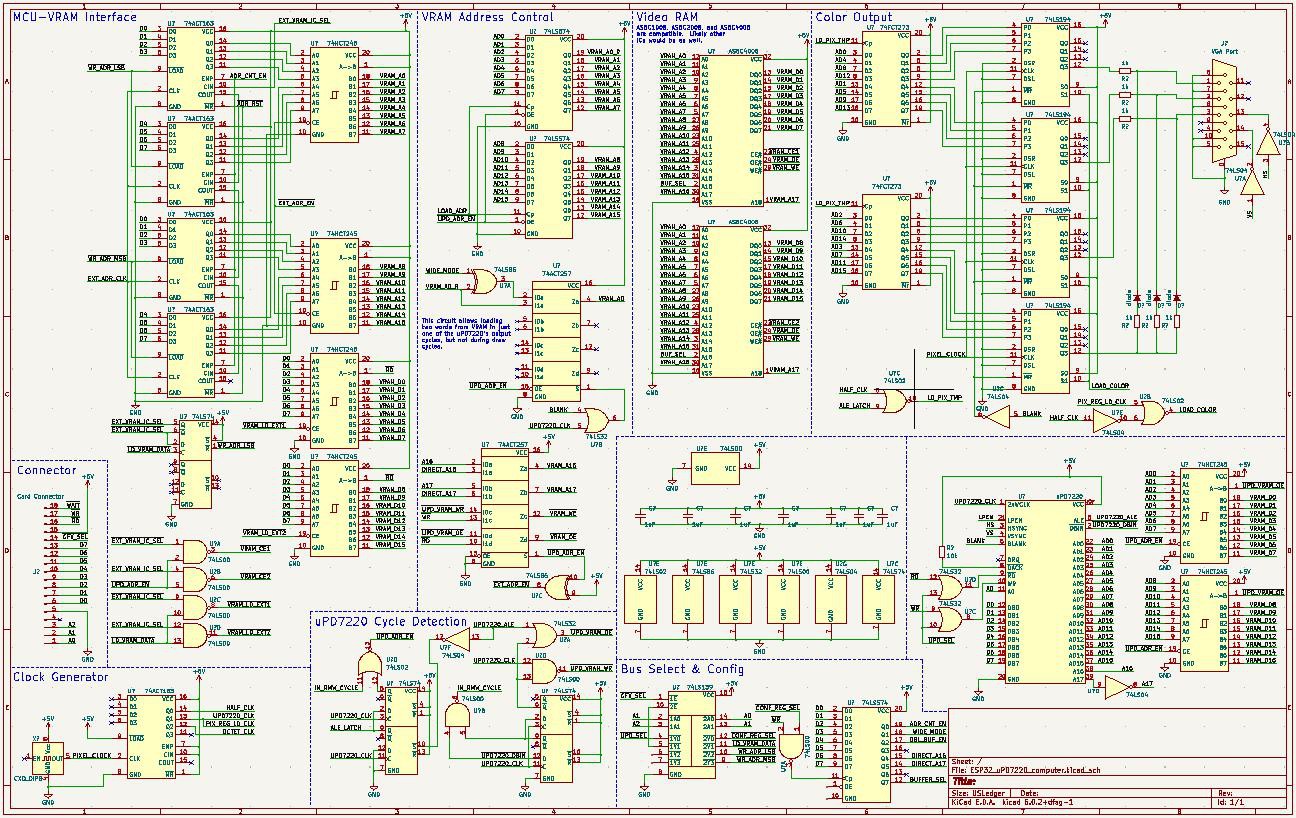
- The CPU can now directly access the VRAM
- I doubled the maximum pixel clock by allowing for uPD7220's wide mode (see last log)
- Added support for double buffering
- I octupled the maximum VRAM to 512KiB from 32KiB. Now we can have larger resolutions with enough RAM left over to double-buffer
Doing all this added a TON of extra logic, so if you compare the above schematic with the schematic of the previous board, this one has at least twice the components, and is far denser.
I had to add a lot of buffers so that the VRAM bus could be shared. This concerns me because it adds a few tens of nanoseconds to certain datapaths, meanwhile I've doubled the maximum VRAM clock speed to 16Mhz. The VRAM uses 55ns alone, and that doesn't count any of the hardware for uPD7220 memory cycle detection, bus sharing logic, etc. So the next step will include checking my datapaths to make sure all the components process fast enough for my clocks.
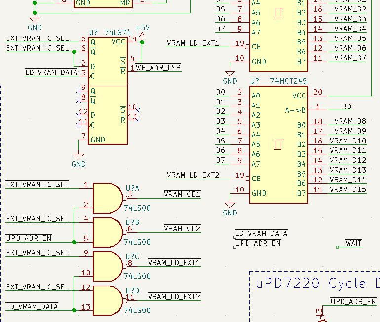 Some of this logic is wrong I think, namely I'm suspicious of the two bottom NAND gates, and I need to add logic for the WAIT line, but this image should give some idea of what the logic is supposed to do. After the main processor writes the lower address byte, the byte-select for the VRAM is reset to zero. Then the processor can write a single byte to the VRAM, which automatically switches the selected byte so the processor can write the other byte. This is done because the VRAM has a 16-bit bus and the processor has an 8-bit bus. Depending on weather the address counting is enabled, the address registers will actually count up to the next word in VRAM, so that the processor can send up to 128KiB of uninterrupted data to VRAM. This is done in-between accesses done by the uPD7220, as the bus is shared, and the uPD7220 gets priority.
The exact behavior of the board's logic is controlled by a special control register I added:
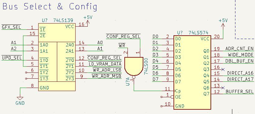 I realize now, looking at this, that I may be able to remove a latch by using A0 for byte select instead of automatically selecting it. Something to think about. Anyway, in the image above you can see that the config register can enable/disable the wide mode logic, control automatic address count, enable or disable double-buffering, to swap buffers, and set A16/A17 for direct VRAM access. The double-buffer enable will make the uPD7220 and processor write to the opposite buffer as the one being displayed, but the buffer still must be manually swapped by the processor.
Anyway, this is where I'm at now. The schematic isn't quite finished, once I finish it and have the board design I'll upload the files to the project.
[edit] bonus: falstad simulation of part of the circuit responsible for loading pixel data from VRAM and clocking it out, which allows wide mode: Simulation
Discussions
Become a Hackaday.io Member
Create an account to leave a comment. Already have an account? Log In.