Close
0%
0%

pcbtc (GaN edition)

The slightly different USB peripheral

Similar projects worth following
When I visited the electronica fair in Germany last year, two things caught my attention that made up a perfect match: The spiral tesla coil by Daniel Eindhoven, displayed at the Elektor booth, and Texas Instruments new Gallium-Nitride switches, advertised for fast switching power converters. Here is the result of what I created since I saw this in November:

A pcb tesla coil that can generate 5cm arcs into the air, powered from my 5V 3A USB C laptop jack. The tesla coil enumerates as a USB MIDI device and can be used from any synthesizer software like LMMS or Ableton. The design is completely open source. I release all software and designs to github so you can build your own coil: https://github.com/lucysrausch/pcbtc
Disclaimer: This is not an easy project. You have to solder eg. fine-pitch QFN. I might sell pre-assembled kits in the future.

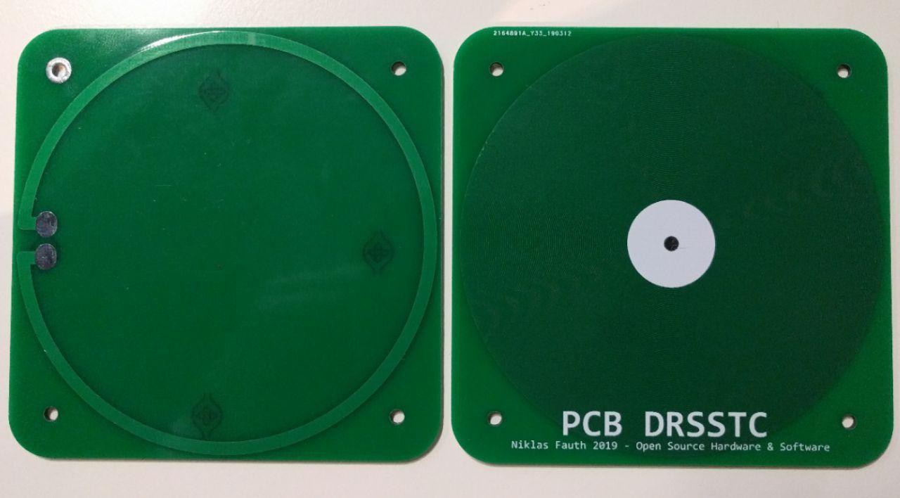
Latest video with three coils controlled via midi:
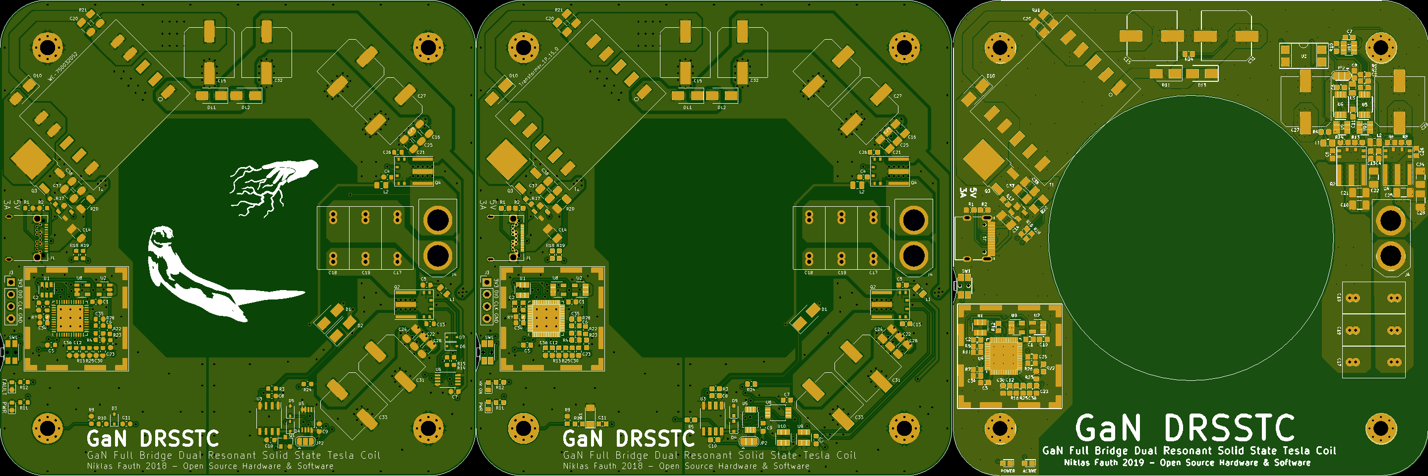

Known bugs (V1.5)

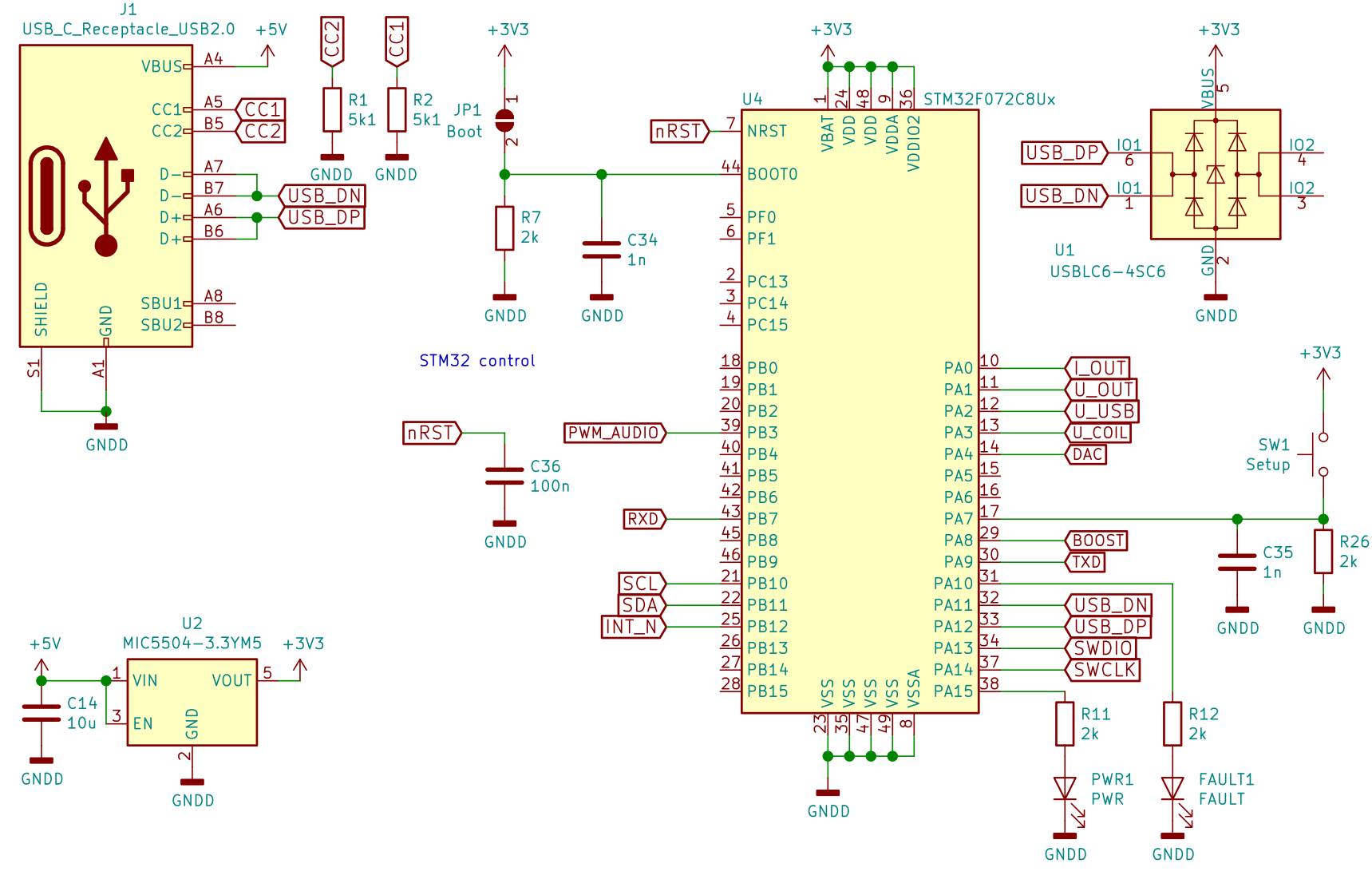
  • Missing pulldown for gatedriver input of the flyback converter. This can cause problems when in DFU mode as the mosfet might switch on permanently, shorting VUSB
  • Missing input decoupling capacitors underneath the LMG5200. Adding additional high-quality 100pF and 100nF ceramic capacitors on the bottom of the pcb improves performance drastically
  • Unknown problem causes GaN module to fail when touching the arcs with the finger or a screwdriver. The reason for this is unknown so far. Maybe EMI, maybe bad layout. Just don't touch the arcs for too long for now. Discharges to air work reliably.

Ideas for V1.6 (or V2.0?)

  • 4 layer design to improve the ground return loop
  • connect the button to both BOOT0 and a GPIO so no additional jumper for initial flashing is required
  • primary current feedback for overcurrent protection and feedback with less propagation delay for better zero current switching, using phase lead compensation
  • physical MIDI input & output jacks
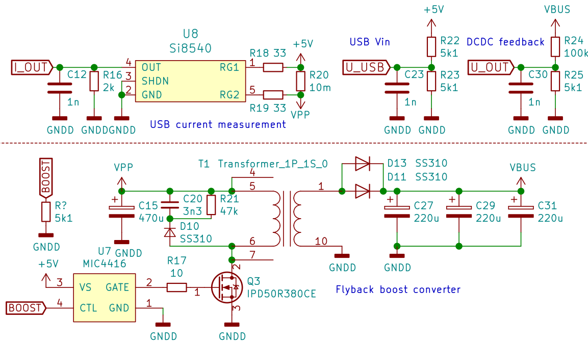
View all 11 components

  • Status update and rebuilds

    Lucy Fauth06/19/2019 at 10:57 0 comments

    It's been some time since I posted something on this project, and I still didn't have time to test V2 even through the pcb have arrived some time ago already. I still got motivation to work on this project through, not least because of the great feedback I got. Thanks!

    Some people even were crazy enough to try rebuilding this project, and all four attempts I'm aware of succeeded with little or no help. This is great, as it means all my documentation is successive and correct.

    I want to give a special shoutout to Zack Goyetche. He built not only one, but four tesla coils, and even made an awesome youtube video about additional theory and the build process.

    So while waiting for some progress on this project, enjoy his video and take it as motivation to build you own tesla coil :)

  • Hardware Design Part 2

    Lucy Fauth05/15/2019 at 17:10 0 comments

    Flyback boost converter

    The flyback converter steps up the 5V input voltage to 40-50V for the GaN full-bridge. As the turn ratio of the tesla coil already is at a max (you can’t have less than one primary winding ;) the only way to get higher output voltages is a higher input voltage. A flyback converter doesn’t work like a traditional transformer, it it much more comparable to a boost converter: The transformer acts as a coupled inductor that stores magnetic energy in the air gap. Independently of the turn ratio, output voltage can reach (theoretically) indefinitely high output voltages. The only difference is that with a well-chosen turn ratio, efficiency can be improved a lot compared to a simply boost topology.

    The PWM for the switching mosfet is generated by the STM32. The STM32 thous has full control of the output voltage, allowing things like slowly ramping up output voltage to not overload USB, software-configurable bridge voltage and potentially QCW-DRSSTC operation.

    Deadtime circuit

    The so-called shoot-through condition happens when both switches in a half-bridge design are conducting simultaneously. This usually doesn’t happen intentionally, it rather happens as a side effect during switching: If you switch on one fet in the exact same moment you switch off the other, due to time delay mismatch it can happen that for a very short period of time, both switches are conducting, usually causing death to both fets. To counteract this unfortunate event, you can add a small amount of time where both fets are off, “break before make”, or, in EE slang, dead-time.

    Even though the LMG5200 already integrate an impressive amount of circuitry, one thing missing is dead-time logic. Texas Instruments arguments that this is an advantage as it gives the designer the freedom of controlling the two individual GaN devices in the half-bridge as they wish. However, it also gives you the freedom to kill both GaN Fets if you turn them on simultaneously.

    I didn’t realize that in my first attempt, and adding dead-time logic was the milestone that lead to the very first sparks from this design. The circuit is pretty easy: Two triple-input AND gates are feed with the feedback signal, one inverted, the other not. Also, enable from the STM32 is applied to both AND gates. The opto-coupler was added to separate the STM32 from the electronics for the tesla coil: As you will learn later, the GND for everything related to driving the LMG5200 is on a separate ground plane, only conneted to power ground through the LMG5200 itself. This is again because the fast switching of the LMG5200 can induce voltage spikes that can lead to unwanted behavior. The opto-coupler is there to connect these to domains without introducing noise to this separated ground plane.

    The third input is the inverted output of each other AND gate: Only one of them can output high at a time, as they are blocking each other. As the signal has to pass through the inverter first to enable the output of the other AND gate, the delay time of the inverting gate is added to the signal as dead-time where both AND gates outputs are low.

    Feedback Signal recovery

    Is is very important for the tesla coil to operate at it’s own resonant frequency. However, this is not a fix value, it heavily changes during operation: Both the amount of metal in the surrending as well as the very arc created by the tesla coil forms an additional capacitance that decreases the resonance frequency. The easiest way to follow these changes is to operate the coil in a self-resonanting mode: The output of the coil is sensed, amplified and feed back to the driving circuit as positive feedback. This causes an undamped oscillation at the resonant frequency.

    There are multiple known attempts to recover this feedback signal. The biggest difference is either it is recovered from the primary resonance circuit or the secondary coil. The easiest way is to sense...

    Read more »

  • Hardware Design Part 1

    Lucy Fauth04/22/2019 at 15:48 0 comments

    As explained earlier, the coil design has an usually high resonance frequency. With traditional Si-MOSFETs it is very hard to build a efficient fullbridge at this frequency. This is mostly because of the high gate charge and switching losses of mosfets the size required for this application.

    It is possible to get sparks even at these frequency, using class-E topology. However, in this mode of operation, the mosfet is in linear mode and has very high power losses (http://www.richieburnett.co.uk/hfsstc.html

    Daniel Eidhoven solved this issue by using traditional bipolar transistors in emitter follower configuration. This allows fast switching and small delay. However, to drive these power transistors, you need another totem-pole driver that outputs a signal with the full output voltage swing. Daniel used a mosfet driver IC for this. With the device he uses he is limited to 32V bridge voltage. Also, bjts are not known for their great efficiency...

    To overcome these issues, GaN and SiC switches require some special gate drivers (eg. with a output voltage of -6 to 10V. The negative voltage helps to bias the gate against mentioned voltage spikes during turn-off.) located as close as possible to the switch.
    Texas Instruments overcame this issue by developing a device with two internal GaN switches in half-bridge configuration that includes all the required low- and highside gate drivers. You can buy these devices since ~6 months for $9 each.

    (http://www.ti.com/lit/ds/symlink/lmg5200.pdf)

    The latest schematics of the full design can be found here: https://github.com/NiklasFauth/pcbtc/blob/master/hardware/schematic_V1.5/pcbtc.pdf

    We can separate the design in five functional blocks:

    • STM32 microcontroller
    • Flyback boost converter
    • Feedback signal recovery
    • Deadtime circuit
    • GaN full bridge

    Revisions

    (three selected design revisions. From left to right: V1.0, 2018-11-22 - no dead time, bad power layout; V1.3, 2018.12.22 - dead time, first arcs, GaNs randomly die after 1-20min; V1.5, 2019-12-04 - good performance, good reliability - still room for optimization ;)


    In total, it took 6 pcb and design revisions to get the current performance and reliability. This is mostly due to the very challenging requirements that come with the use of GaN switches. Some pcb revision could have been avoided if I would have followed the recommendations in the datasheet in the first place. Usually, you can interpret design guidelines and maximum ratings as "recommendations" - this is definitely not the case when it comes to GaN and SiC design. When TI writes about placing components "as close as possible" like they do on page 10, 13, 14, 15 and 16 of the datasheet - 8 times in total! - they really, really mean it like that. "Close" does not mean "nearby". "Close" does not mean "right next to it". "Close", in terms of low parasitic inductance, means: on the opposite of the board, right under the according pads, connected with as many vias as you can stick in there.

    I had to learn this the hard way - I might have killed 10 LMG5200 modules because I though I knew better. But more about layout considerations, later. Let's start with the easy stuff:

    STM32 microcontroller

    (yes, it looks like USB DN and DP are shorted - the schematic symbol is for a USBLC6-2SC6, but I'm using a USBLC6-4SC6. I'll fix this soon but no worries, it's just graphical)

    There is nothing too special about this. I used the STM32F072 for this project, one of my favorite parts from the STM32 series. The STM32F072 is cheap, has a proper ARM M0 core, and supports crystalless USB operation by using clock recovery / syncing from the USB frames. So you get a decent Micro with USB and lot's of STMs powerful timer peripherals for under $1 that requires minimal external components. I used the QFN version because I find it much easier to solder than QFP.

    Also, the STM32F072 has a DFU...

    Read more »

  • The coil design

    Lucy Fauth04/21/2019 at 21:32 0 comments

    I don't want to talk too much about how tesla coils (https://en.wikipedia.org/wiki/Tesla_coil), and more specifically dual resonance solid state tesla coils (DRSSTC) work, as there already is lots of great literature on that (https://www.easternvoltageresearch.com/documents/book_drsstcpreview.pdf).

    Basically, a tesla coil consists of an air-coupled transformer with a very high turn ratio. Low AC input voltage is transformed to high AC voltage, that is, in case of the dual resonance system, additionally amplified by electrical resonance effects. This high voltage is concentrated at a small tip, the breakout point, where the local field strength it high enough to ionize the air and create the arc.

    We can separate the design in two parts, the passive transformer itself, and the electronics driving it. Let's start with the transformer first, as this explains some of the design choices for the driving part.

    Most of you probably already have seen a tesla coil

    (cc by Johannes Müllers)

    These devices are usually smaller than 1m in height, but almost always bigger than 10cm. This has a very good reason: As the transformer has no core other than air, and there is some limit to the number of turns the coil can has (usually in the range 200-1000), the secondary resonance frequency (the frequency of the LC oscillator defined by the inductance of the secundary windings and the capacitance of then top electrode to ground) is only defined by geometry. For a 30cm coil, this would be in the range of 200-300kHz.

    Here lies the first problem: Building bigger tesla coils is actually easier than a very small one. For DRSSTCs, the power electronics driving the transformer is usually based on IGBT switches, sometimes MOSFETs. But even with very modern Si-based switches, the switching losses increase massively at a frequency  >1MHz. For reference, most motor controllers use 15-25kHz. Your laptops power supply no more than 200kHz. My coil design is at 2.6Mhz.

    Usually, you use isolated magnet wire around a plastic tube for the secondary coil. This has the obvious advantage that as the voltage increases towards the top of the coil, also the distance towards the sensitive power electronics and primary windings on the bottom increases. However, manufacturing these coils is a lot of hand work. You can't just buy them in arbitrary quantities.

    PCBs, however, have become super cheap. You can get 10pcs 100x100mm dual layer pcbs for $5 at your Chinese manufacturer of choice. With 5mil tracing and 5mil spacing as required by most manufacturers, this gives you 190 turns on a 100x100mm pcb.

    (left: bottom side with single primary winding, right: secondary winding with 190 turns)

    There is nothing special really to these coils. It's really just a huge spiral going from the outside to the inside. I placed a circle of white silkscreen in the center the increase isolation a bit. The primary winding is a single turn. I also tried two and three turns (yes, I had to order new pcbs to test this, but it's just $5 so why not?) but as the secondary turns are already so low (190), you want to get maximum transformation ration. The primary winding is connected with pads to a XT60 high current connector, and the secundary winding has a pad in the center and a plated mounting hole on the low voltage side to connect the base point to the electronics for signal recovery and grounding.

    Unfortunately, I was not able to create the gerbers for this in KiCAD as it interpolates circles with very bad resolution. I tried a svg to gerber converter but that also failed. I ended up booting my Windows VM and just used Altium Designer to create the files. Luckily, I did not have to change these files a lot, and you can find the gerbers on GitHub.

    I ordered my coils at jlcpcb. They rejected the design because it failed the audit. Technically the design is perfectly within spec, however it is somewhat relatable: You're requesting...

    Read more »

View all 4 project logs

Enjoy this project?

Share

Discussions

Paul Andrews wrote 10/30/2019 at 22:13 point

I see you added some build instructions to github, and the version of the PCB in that is 1.7. Is that version checked in to github?

  Are you sure? yes | no

Muth wrote 11/07/2019 at 11:29 point

I got recently everything to build it. I made a first one, using the V1.6 board. Other than placement, the only differences I can see from the pictures on the instructions are the STM32 package, and an additional 220uF capacitor on the 50V VBUS.

I had to be careful to choose the capacitor voltage, Vbus is 50V. So for the 10uF on 1206 size, 50V seems to be the maximum existing.

The one I built works, but the 50V flyback boost converter is struggling to maintain the voltage. When you play a tone, the Vbus capacitors are emptied in ~200ms. Then it takes roughly a second to recover. During this recovery time the duty cycle of the mosfet is 50%, but something like "only" 1.5A is taken from the 5V. I don't know if this should be bigger. I'm using a big lab power supply on the 5V (36A), so it is not the usb limitation.

  Are you sure? yes | no

Muth wrote 11/08/2019 at 16:37 point

Ah yes, and there is the transformer which is different. The one in V1.6 is 10uH while the one on the V1.7 is 37uH. Maybe I should look at this for the Vpp drop.

  Are you sure? yes | no

Tom Meehan wrote 08/26/2019 at 02:53 point

EXCELLENT, I love Tesla Coil projects and this is great!

  Are you sure? yes | no

profdc9 wrote 05/02/2019 at 00:29 point

Hello Niklaus,

I was thinking about implementing something like this but I found your project and it seems you are already doing an excellent job.  I had a couple of things you may be interested in.

I designed a Theremin which I will use to control my Tesla coil.  You can find it on github here:

https://github.com/profdc9/MCTheremin

It may be cool to demonstrate controlling your tabletop tesla coil.

I have been using the Bluepill STM32F103C8T6 because of its low cost and it does not require QFP soldering skills, already being mounted on the board.  Also, it comes with many parts already mounted and a USB connection so that reduces part count.  It doesn't take much board space because you can place components under the Bluepill.  Something to consider?  I try to design my kits for newbies and have avoided tiny parts where I can.

Also, I designed a spiral coil in Kicad.  I had to hack Kicad a bit to make it work and use an external script to generate the paths, but the coil is smooth and well-interpolated.

Excellent project and I will keep an eye on it.

Dan

https://hackaday.io/hacker/378100-profdc9

  Are you sure? yes | no

Similar Projects

Does this project spark your interest?

Become a member to follow this project and never miss any updates