Close
0%
0%

350 Watt True Sine Inverter

Functional design revision of the prototype TS350.

Similar projects worth following
The TS350R1 builds on my experience from the prototype and is a practical & working design that fits in a standard extruded aluminum case. When powered from a +13-16V DC source it will deliver a low distortion 60Hz sine wave output of 350 VA continuous at 110 VAC in ambient temperatures up to about +40C. In boost mode it will supply up to 400 VA (input voltage & thermally limited). Likewise it handles inrush currents & transients and will tolerate a dead short on the output.

It will work with input voltages down to about 11V DC and automatically derates the output. It includes a front-panel LED meter to indicate the relative load and fault codes. Protections include a fused input, under/over-volt, over-current / overload, and overheat. The AC output is fully isolated. It is cooled by internal, temperature controlled fans.

Anderson PowerPole jacks are used to connect input power. Like some of my other projects, this one includes a micro-USB service port.

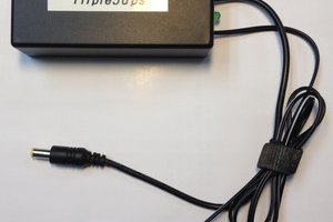
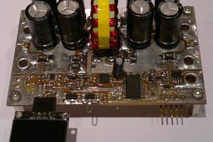
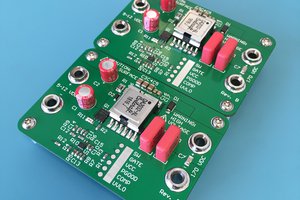
Specifications (as pictured)

  • Input voltage:  11-16 volts DC
  • Operating temperature:  -20C - +40C
  • Maximum continuous input current:  45 amps
  • Idle current:  420mA
  • Output voltage:  100-120 volts AC RMS (110V AC RMS nominal)
  • Output frequency:  60Hz, +/- 0.5Hz
  • Maximum output power:  400 VA
  • Continuous output power:  350 VA
  • Total Harmonic Distortion (THD):  <5%
  • Efficiency:  81%
  • Galvanic isolation between DC input & AC output
  • Protections:
    • 60A input fuse
    • Input under/over voltage
    • Over-current / short
    • Overload
    • Overheat
  • Dimensions:  L=203mm (8"), W=144mm (5.7"), H=68mm (2.67")
  • Weight:  ~ 1.36kg (3lbs)

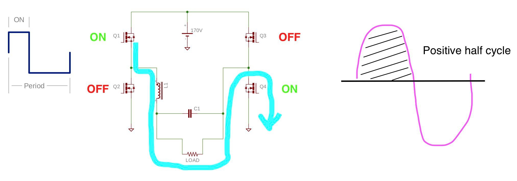
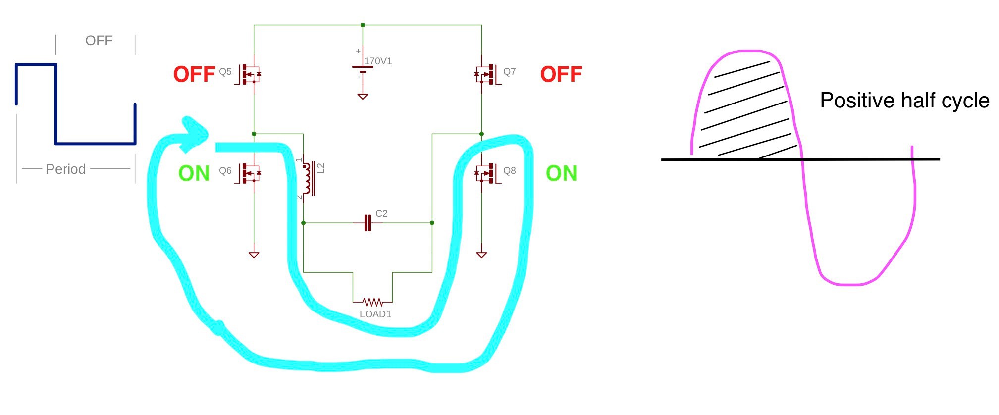
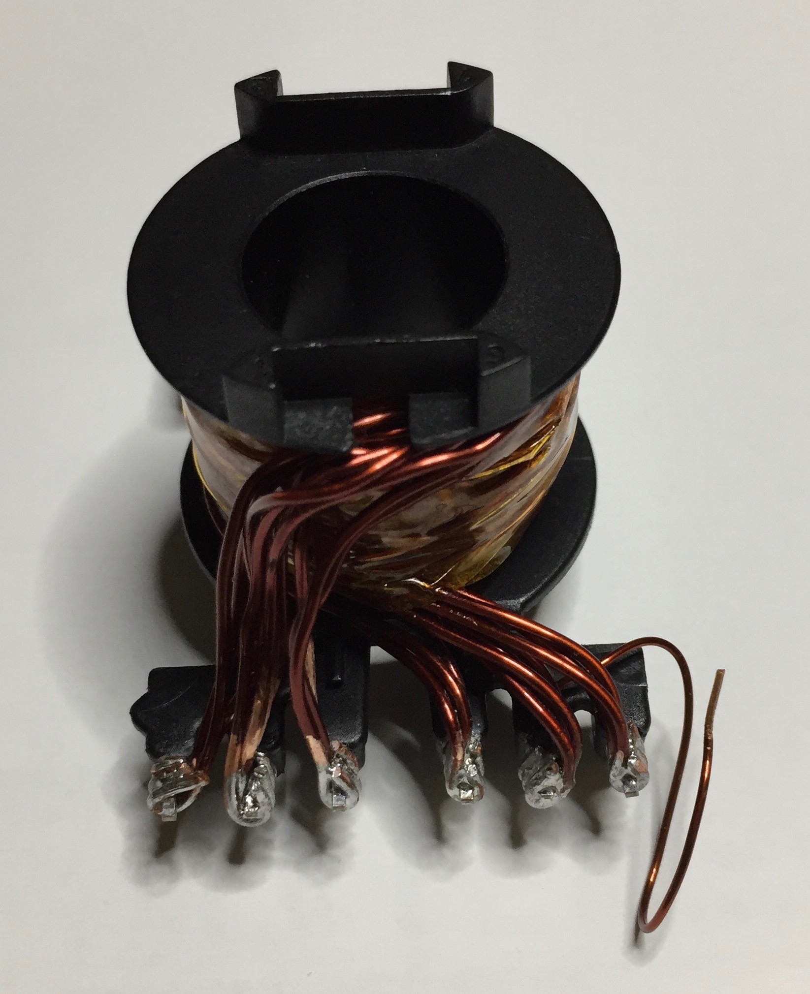
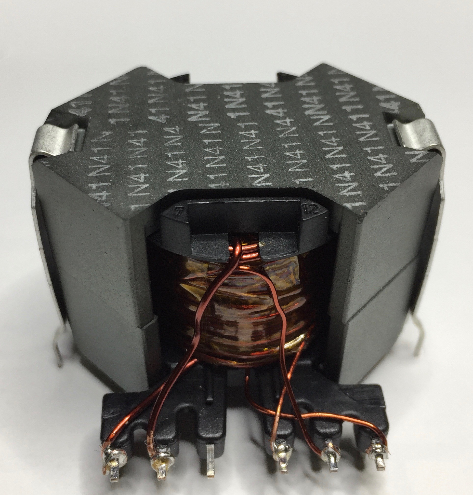
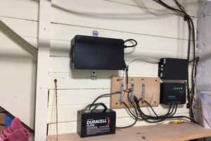
This project is done.  If you do build it please read thru all the instructions first.  I recommend that you build from the input section forward:  power -> start -> controller -> inverter -> transformer & supplies -> sine.

CAUTION:  high voltages, currents, and temperatures exist in this design.

ts350r1-magnetics.zip

Transformer & output inductor design / analysis data.

Zip Archive - 131.98 kB - 05/10/2019 at 13:53

Download

ts350r1-excel.zip

MS Excel design workbooks.

Zip Archive - 273.70 kB - 05/08/2019 at 16:54

Download

binary.h

C include file common to both controllers.

h - 883.00 bytes - 05/08/2019 at 16:53

Download

ts350r1-firmware-sine-v2_b14.zip

C source for sine controller (Microchip MPLAB).

Zip Archive - 25.67 kB - 05/08/2019 at 16:50

Download

ts350r1-firmware-controller-v2_b50.zip

C source for main controller (Microchip MPLAB).

Zip Archive - 39.46 kB - 05/08/2019 at 16:50

Download

View all 10 files

  • Sine Section

    Brian Cornell08/19/2019 at 00:09 0 comments

    Theory of operation

    Much of this is abbreviated from the TS50 project so you can get more detail there.  The sine bridge is an implementation of Direct Digital Synthesis (DDS).  The controller produces a set of fixed frequency, duty-cycle varying drive signals connected to an H-bridge that send the modulated high-voltage square wave thru a set of LC filters to produce a low distortion 60Hz sine wave.

    The bridge operates at 48kHz which allows for a sine pattern with 200 discrete values per quarter sine.  Each value represents the time equivalent of a sine angle from 0 - 90 degrees.  The controller ‘plays’ the pattern forward & backward for each half sine and then repeats the process for 180 - 360 degrees.

    Electrically, the H-bridge functions a bit different from one driving a transformer.

    During a given half cycle the low-side switch Q4 remains on (no switching) which connects the load to the high voltage supply negative pole.  When the high side switch, Q1, is on, inductor L1 is charging and current flows thru the load to the negative supply pole.

    When Q1 turns off L1 reverses polarity to maintain current flow.  To close the circuit Q2 turns on.  Current no longer returns to the high voltage supply but instead uses the ground plane to flow thru Q2 and return to the negative node of the inductor.

    This process repeats for one half sine cycle and then reverses with the other half of the bridge performing the switching.  Although the diagrams only show a single LC filter, the TS350r1 has one for each leg and functions the same.  The architecture could be thought of as two alternating and parallel buck converters.

    Power Supplies
    The sine section has three supplies.  The Vcc supply is derived from a full-bridge rectifier on the transformer auxiliary winding and provides 13V via LDO U403.  Vcc powers the gate drive and bootstrap circuits.  Vdd provides the 5V logic supply for the controller, temperature sense, and communication isolator.  An unregulated tap is also taken directly from the rectified transformer auxiliary that is used by the controller as a proxy for the high voltage supply (and is spared the dissipation of a resistive voltage divider).

    The high voltage supply consists of a full bridge rectifier and powers the H-bridge.  Heat sinking is required, so to conserve space dual common anode/cathode TO220 packages are used.  Three lower-value capacitors are placed in parallel to provide bulk capacitance.  This allows for a lower maximum mounting height with no trade-off in PCB space based on the layout.  The cost is just slightly more for three smaller vs. one big one.

    With a two stage inverter design such as this, more capacitance for the high voltage supply isn’t necessarily better.  It costs more, takes up a lot of space, and can complicate short circuit hardening for the H-bridge.  It also puts more strain on the boost stage, both at startup and to keep it charged when under heavy load.  This design’s transformer has poor regulation so the bulk capacitance helps reduce the sag to keep the minimum AC RMS voltage a bit higher than it would otherwise be.

    Controller Card
    The controller card houses the gate drivers and MCU.  It’s physical design is very similar to the inverter:  right angle 100mil pins, vertical mount.  This allows for a more compact design and small gate drive loops.

    The gate drivers are the same component that is used for the inverter.  And, as with the inverter section they allowed for minimal components to manage parasitics.  Even though the controller to gate drive signal lines behave as a lumped system, the traces lengths are matched to ensure clean timing.

    The MCU’s main job is DDS pattern generation which includes a crude form of voltage regulation.  Secondarily it monitors the bridge temperature and turns the AC output on & off in response to assertion of the CMD pin.

    The...

    Read more »

  • Controller

    Brian Cornell08/01/2019 at 20:22 0 comments

    In other logs I’ve written about how specific aspects of the controller design integrate with the hardware so this one explains the architecture in more detail.

    Overview

    The controller is a Microchip PIC16F1776 8-bit microcontroller (MCU) with 16KB of flash program memory and 1KB of static RAM.  The system oscillator is set to 16MHz with an instruction speed of 4MHz.  The firmware is written in ANSI C and compiled in ‘Pro’ mode using the XC8 compiler.  

    On-board peripherals handle all real-time control (bridge, current protection, ADC, etc.) so, the MCU’s 4 MIPS is adequate and the firmware uses a polled architecture.  Its main job is to provide operating envelope management and communicate status via the front panel LEDs or service port.

    Most of the source code is well documented and supplements what’s presented here.  You’ll notice that the compiled code size is large - this is to support the console interface.

    Boot Process
    The boot process is divided into three stages:

    1. NVM / CPU validation
    2. Peripheral configuration
    3. Inverter startup

    At boot the Power Control (PCON) and CPU status (STATUS) registers are evaluated to determine if the boot was due to a watchdog or CPU trap (e.g. stack).  If any of these conditions evaluate TRUE the boot will complete with error and a status code set on the front panel LEDs.  The inverter will not start without power cycling which is done for safety.

    A row of program flash is used to store the system configuration and the last word contains the checksum for the row.  This value is compared to the dynamically generated checksum.  Similarly, a mismatch causes the boot to complete with error, set an LED status code, and prevent normal startup without power cycling.

    In both of the above situations the status code will be written to NVM.  In the case of the checksum error this has a self healing effect: the entire row is rewritten with default values which should reset the checksum unless there’s a flash memory failure.  Also, while the inverter won’t start, the service port is active and can be used to troubleshoot.

    The second boot step is peripheral configuration.  This starts with loading configurable parameters from NVM and then configuring the on-board peripherals.  No validations are performed during this step.

    Inverter startup is performed in the run-time loop.  Once the data collection block validates the operating environment (e.g.  temp, current, voltages), control proceeds to the boot (autostart) block.  The NVM configuration directs what happens:  the unit can remain stopped, start only the inverter section, or start inverter & sine sections.  When the inverter is started several things happen:

    1. The bootstrap capacitors are charged.  High-side shorts are also detected.
    2. A soft-start function slowly increases the duty cycle from 0 to the set value to reduce component stress and EMI.
    3. The steady state duty cycle is monitored to detect shorts (or other HW malfunctions that would reduce duty cycle).

    If NVM also directs the sine section to start then the sine command pin (PIN_O_SINE) is asserted and the acknowledgment pin (PIN_I_SINE) is monitored to confirm start within the timeout period.

    Any error encountered during startup sets the unit to a stopped state with the front panel LEDs displaying an error code.  A power cycle is required to restart.

    Run Loop
    The run loop is a waterfall design and  consists of several discrete conditional sections that execute sequentially:

    • Watchdog timer:  this is reset at the top of the loop.
    • Data collection:  system voltages, temperatures, and current.  Many of these are averaged over several samples to eliminate noise and ripple.  These values are used in subsequent processing blocks.
    • Thermal management:  turns fans on & off based on inverter temperature and thresholds set in NVM.  A ‘feature’ of this block is that it can be used...
    Read more »

  • Input Power Management

    Brian Cornell05/25/2019 at 17:25 0 comments

    This covers the input power connections, control & protections, and inverter auxiliary supplies.

    In keeping with the design philosophy that minimizes the unit’s dependency on the enclosure, 45A Anderson PowerPoles are used to connect to a power source.  They are quite effective in providing low connection impedance and ease of use.  I do have concern for the long-term mechanical durability of the PCB mounts, particularly with a 30mil board, since the insertion force is considerable.  This is why a strap is placed around the connector.  Note that Anderson offers mounting “wings” for this application but they triple the width of the connector footprint.

    The entire unit is fuse protected with two paralleled 30A automotive-style MINI fuses.  These are the highest amperage value available in that form factor and overall occupy the smallest space.  The fuses connect to the input of the Solid State Relay (SSR) and power switch S201.  The switch is a low current (rated 5A) that powers the start circuit and auxiliary supply.  Switching of power to the inverter bridge is handled by the SSR.  This scheme avoids the use of a bulky high-current mechanical switch, enables inrush management, and eliminates sparks as a potential ignition source.

    The start (switched) circuit is protected by a PCB mounted 1.6A fuse (F203).  It is intended to disable the unit if an internal short develops, or connected with reverse polarity or to excessive voltage.  As described in the Overview of Operation, the start circuit’s main function is to provide over-volt protection and that detail won’t be repeated here.  Essentially it consists of pass transistor Q205 and provides two levels of over-volt protection.  The first level is non-destructive and disables the unit if connected to a source in excess of 16V but less than 30V.  The second layer engages a zener shunt that opens F203.

    U201 is a 6W SMPS in a DIP package.  It provides Vcc and, via LDO U202, Vdd supplies to the inverter section.  It is connected to the output of pass transistor Q205.  The auxiliary supply also powers the cooling fans which are switched by Q207 via controller U101.

    The SSR consists of two paralleled MOSFETs, Q202 & Q204, that connect the inverter bridge to the power source.  During operation their combined Rds(on) at operating temperatures ~ 90C is less than 4mΩ.  When the unit is first powered on they are off and the bridge capacitors, C301-4, are charged via R210.  D204 prevents power from the inverter bridge from powering the auxiliary supply when the unit is switched off.

    The SSR is connected to the positive input and does not provide reverse polarity protection.  The prototype had this but was eliminated to conserve space and reduce cost.  The SSR requires a floating gate drive which is accomplished with a simple flyback circuit.  It is driven directly by controller U101 with a fixed duty cycle, 100kHz PWM.  It provides a stable 15V drive with ~ 0.5V of ripple and a turn-on time less than 100uS.

    The inverter bridge contains substantial bulk capacitance - about 4800uF.  This is necessary since the input impedance is unknown:  connection lead length, wire gauge, and impedance of the source.  More capacitance would be better but cost & space become an issue.  The design criteria expects lead lengths of about a meter using 10AWG wire connected to a 12V automotive style power system.  Under these conditions this bulk capacitance can source full current (~48A) for a switching cycle and will keep the switching frequency ripple under 200mV at full load.  Line frequency (60Hz) ripple will be about one volt and is unavoidable.

    Ignoring the impedance (e.g. cut-off frequency) of the connection wiring and given:

                (A * s) / V = C          ...

    Read more »

  • Inverter Gate Drive and Switching

    Brian Cornell05/21/2019 at 21:04 0 comments

    I’ve written about the inverter’s transformer design and current management scheme in other logs so I figured I round it off with one on the gate drive and transistors.

    Layout

    A big goal in this design was a reduced layout in terms of both physical space and electrical distance.  Going vertical seemed like a sensible way to do this.  It has the added advantage of placing the low power & logic components on a separate board thereby reducing thermal stress.

    This part of the design has worked well.  The 100mil right-angle mounting pins aren't the best for density but they do provide good support.  A separate board allows for potential reuse in other designs and for upgrades without obsoleting the base design.  The main (power) board can also use heavier copper for the high currents without creating problems for the close traces required of the logic components.

    Gate Drive
    International Rectifier’s IRS21864, monolithic, half-bridge gate driver is used.  It’s actually a high voltage model and is used on the sine section as well.  It’s used here to reduce the parts mix and because it otherwise supports a 4A gate drive source/sink and is single supply.  I also selected it because of prior experience with other parts from this family.  They are very durable, have good noise immunity, and tolerate ridiculous amounts of ground bounce.  Ground bounce refers to refer to the phenomenon of Vs and COM below ground.  Both are due to high di/dt, transformer flyback, and the parasitic inductances (e.g. transistor leads, PCB traces, etc.).

    Vs below ground refers to the gate driver’s Vs pin that is connected to the center leg of the half-bridge.  During turn-off of the low side the transformer’s primary reverses polarity by flyback action.  Vs will move below ground by the MOSFET body diodes’s Vf plus series voltages induced by the parasitics and the di/dt.  COM below ground refers to the gate driver’s COM pin that is connected to the source of the low-side MOSFET.  This is the reverse of Vs:  during turn-off the parasitic inductances in series with the transistor and the star ground reverse polarity and induce a flyback voltage based on the di/dt.

    It doesn’t take much parasitic inductance to wreak havoc.  Given that the instantaneous voltage across an inductor is:

        L * (di / dt) = V            (1)

    Conservatively assuming that the total parasitic inductance of the source-ground is 7nH (a standard hight mounted TO-220 could have this much), using the Iin_max (current in, max) value for this design of 45A, and a turn-off / fall time of 84nS (ref. ‘mosfet-inv’ tab of design workbook):

        7nH * (45 / 84nS) = 3.75V    (2)

    I haven’t done formal measurements on the design but I’m sure that they are higher than this and is a key reason why I didn’t use low-side current sensing in this design.  IR guarantees the gate driver operational with COM up to 5V below ground.  Beyond this damage occurs.  This is due to the internal diode structures.

    The ground margin on Vs is higher and depends on the gate driver’s Vcc.  In this design the margin is 13v:

        Max Vcc = 20V
        - Design Vcc = 12V
        Vcc Margin = 8V
        + Ground Margin = 5V

        Total Margin = 13V

    The high-side driver will latch-up when Vs exceeds 5V below ground but won’t incur damage until the total margin is exceeded.  The TS350 is likely exceeding 5V but it isn’t a problem since the high-side transistor is off.

    Fortunately the design didn’t require special compensation to protect from these conditions and resulted in a simple design.  The gate drive resistors are sized to minimize switching times within the source/sink limits of the gate drivers.  Current limit resistors in the bootstrap charge circuit protect...

    Read more »

  • Current Sense Post Mortem

    Brian Cornell05/13/2019 at 18:26 0 comments

    There is a problem with the layout of the current sense circuit that distorts the ‘B’ side signal.  Here is a trace: 


    Channel 1 is the sense signal at the gate driver card pin connecting to the main board.  Channel 3 is the ‘A’ side drive signal, so when 3 is low the sense signal is coming from the ‘B’ side of the bridge.  Amazingly, it doesn’t appear to effect the safe operation of the unit.  Below is a trace of over-current limiting prompted by a surge event on the sine output:


    Channel 1 is the gate drive for the ‘A’ side and channel 4 is ‘B’.  Channel 2 is the current sense signal from the gate card pin.  Note the delay and subsequent higher DC for the ‘B’ side; but still short enough to protect the transistors.

    Instruction ten describes a fix to improve the B signal and it’s highly recommended that you do this.  Below is the output from the sense pin with the modification.


    So what happened?  Poor layout is to blame:  the circulating currents in the bridge traces interfere with the signal.  Using discrete wires avoids this.

    A proper fix requires placing the amplifier closer to the sense resistors and at the same time keeping the distance from the amplifier output to the controller short as well.  As explained in the log on the general design problem that is essentially a redesign.

  • Current Monitoring and Over-Current Protection

    Brian Cornell05/13/2019 at 18:22 0 comments

    The TS350R1 employs a discrete, high-side current sense circuit in the inverter primary that is the basis for all over-current protection & monitoring in the unit.  Reference the main & inverter gate drive schematics for details.

    The current signal is derived from a pair of 3mΩ (R302, R303) sense resistors that create a 1.5mV/Amp voltage drop across them.  A resistor solution was chosen due to its compact size and low cost.  They are placed in a high-side configuration due to the high currents and to provide better protection for the bridge.  Low-side circuits can’t detect shorts occurring upstream and can contribute to ground bounce related problems for the gate drivers.

    The challenge with high-side sensing is that it isn’t ground referenced so the conditioning circuit must operate from an floating supply or be capable of handling the common mode voltage.  Since isolation isn’t practical the TI OPA197 (U2) is used.  It allows for rail-rail inputs and supports slew rates up to 20V/uS which is satisfactory for per-cycle current limiting.  It is configured as a differential amplifier.  R4 & R5 in conjunction with D2 & D3 provide input protection from voltage spikes.  R4 & R6 set the gain at 10 and Q1 level shifts the output (removes the CM voltage) for direct consumption by controller U101.

    The controller processes the current sense signal to provide per-cycle [SOA] protection for the bridge MOSFETs and to perform overall power management thru two distinct hardware pathways using on-chip peripherals.


    MOSFET SOA Protection
    Per-cycle protection uses DAC1 to provide a reference voltage to comparator CM2.  The reference voltage is set to a value high enough (140A) to support the significant currents required of equipment startup surges but still within the MOSFET’s Safe Operating Area.  CM2 compares the sense value to this reference and produces a H->L transition that is gated thru logic cell CLC3 to a Falling Event input of the COG (Complementary Output Generator).  A transition immediately terminates the gate drive for that side of the bridge for that cycle.

    The role of CLC3, along with PWM11, is to provide a blanking function at the beginning of each half cycle.  Blanking prevents a premature termination of the gate drive and is set to a few hundred nano-seconds (defined by the DC of PWM11).  This is necessary because of the inherent noise in the current sense signal.  Noise is a problem for all sense circuits based on shunt resistors but it is more significant in high current, high frequency applications due to parasitic inductance and poor signal to noise ratios.

    Current Averaging
    The current sense signal is also connected to the non-inverting input of opamp OPA2 which is configured as a voltage follower.  This is necessary because of the relatively high impedance of the current sense circuit’s output and, most importantly, for OPA2’s tristate feature.  Tristate, along with C1 (C102 on the main schematic) form a sample & hold circuit that averages the current sense signal from both sides of the bridge and allows the controller to derive RMS current.  CLC2 gates OPA2’s output to ensure that it is only passing a signal when the bridge is active.

    The voltage read from C1 represents an averaged value of the sense signal but it reads high.  This is because the sense circuit delivers an exaggerated slope with a large spike (parasitics) at the end of each cycle which inflates the measured S&H voltage.  Since the controller has limited processing bandwidth a linear coefficient is applied to reduce the read current to obtain a value that is +/- 1.5A of the actual RMS value.

    The controller multiplies this RMS current value with the inverter’s input voltage to estimate the input power and uses this to perform load management.  The power value drives the front panel LED meter and overload shutdown.

    Overload and Power Management...

    Read more »

  • Inverter Design

    Brian Cornell05/10/2019 at 20:25 0 comments

    At the core of all power supplies is a transformer.  It is central to the design and dictates the form and function of everything around it.  A home brew design imposes additional requirements.  Without specialized tooling and winding materials (e.g. Litz or foil wire, etc.) the design must also be constructible.  Given this, my criteria were that the transformer must be:

    • Manufacturable
    • Efficient
    • Simple
    • Reliable

    From earlier work I knew that a center tap secondary is not practical due to the voltage gradient and turn-turn capacitance.

    In a center tap secondary, the voltage measured across the legs is twice the output voltage.  So a 200V secondary actually has 400V across the entire winding.  In high frequency transformers this, combined with the turn-turn capacitance becomes a serious problem that results in significant ringing.  Here’s an example:


    Note the cursor value and the scale for channel 3 - 100V!  Professionals get around this with lower capacitance magnet wire and special winding techniques that can only be done by machine (e.g. Bank).

    Which is a shame since a center tap requires only two rectifiers instead of four.  That may not seem significant but consider the consequences:  space, dissipation, materials.  In this design if a CT were viable I could have ditched the heatsink and likely used two SMD diodes saving space & halving the dissipation.

    Decision 1:  single winding secondary.

    A center tap primary is possible and that would allow the use of a half-bridge - again saving significant space and halving dissipation.  But there are drawbacks:

    • Window utilization is poor - each half winding is only doing work half time.
    • A larger core size would likely be required given the size of the winding - 2 turns of 20 AWG 10 strands becomes 4 turns.
    • Terminating the center tap would be problematic.
    • Greater chance of staircase saturation:  any imbalance in each half winding (due to construction) creates a flux imbalance which over successive cycles walks the core into saturation.

    Decision 2:  single winding primary.

    An inverter acting as an AC power source must be capable of handling large currents and supporting surge power well beyond their continuous rating.  To do this the transformer must have a high power density and this requires operating it across the full BH loop in quadrants 1 & 3.


    This is related to the single vs. center-tap primary discussion but emphasizes the power handling requirement of the transformer.  To operate the transformer in this manner requires either a half or full bridge; but the prior discussion already discounted the half bridge due to manufacture concerns.

    Decision 3:  full bridge.

    Most switching power supplies regulate thru some form of modulation - either the switching frequency, duty cycle, or both.  Without a center tap secondary the conventional approach to regulation via the use of an output inductor to prevent the transformer core from resetting during off time isn’t practical.  A current fed primary topology is a possibility but adds inductors & switches, introduces more losses, complicates the design, requires more space.

    Decision 4:  no regulation.

    These decisions support the design criteria:  a design that is manufacturable, simple, reliable, and (theoretically) efficient.  The transformer can be operated at a high, constant, duty cycle, utilizing the full BH loop and achieving good power density.  The complexity of a control loop is eliminated.  But this shifts some burden to the rest of the design, both in front of and behind the transformer:

    • A full bridge will be used, doubling the space requirements and losses.
    • A full bridge rectifier is required, also doubling the space requirements and losses.
    • The secondaries will track the input voltage according to their turns ratio and both limit the...
    Read more »

  • The Specific Design Problem

    Brian Cornell05/09/2019 at 19:53 0 comments

    I did a poor job on the systems engineering for this project.  I spent a lot of time on specific problems like the layout of the inverter bridge, rectifier switching losses, heat sinks, firmware, etc. but I was too myopic.  I didn’t bring it all together early enough in the design and this resulted in two major deficiencies.

    Thermal management.  I spent much time modeling heatsinks’ thermal performance, tab insulator materials, mounting height considerations to minimize parasitics and - key - the coefficients of each transistor on the dual sinks.  But I stopped there:  I compartmentalized the thermal models and did not establish the coefficients of adjacent areas or consider the entire system given hot air would be circulating in an enclosure.

    I should have mocked-up the full layout with all key heat sources to establish coefficients and determine the size fans it would need.  The as-built dissipates ~ 68 watts of heat at full load.  Had I better established this early on I would have changed fan positions and sizing or maybe the entire design.  I was fortunate that I had a convenient spot, and the power budget on the auxiliary supply, to add a third fan.

    An early design goal was, aside from board size, for the unit to be enclosure agnostic.  That’s how the pull/push arrangement for the fans on the board came to be.  I realize now that in a design dealing with this much dissipation that the enclosure and the gear going in it are inextricably linked.  An ah-ha related to this is that a fan must be positioned at the enclosure to ambient interface to ensure air is forced in or out of the unit.  Otherwise internal fans will only be moving hot air around.

    I also might have thought twice about trying to get this much power out of it.  A two layer, two ounce PCB is woefully inadequate to handle this much current.  Traces turn into copper pours, grabbing more space and reducing layout efficiency.  Sometimes both layers must be used wasting even more.  In spite of a very generous layout for the inverter primary it is dissipating almost five watts.  That might not sound like much against the total losses but it is concentrated around other high dissipators and contributes significant heat stress.

    AC Voltage Regulation.  The sine controller has eight DDS sine patterns stored in flash and selects one based on the transformer’s auxiliary supply voltage (a proxy for the HV supply).  It does a good job of keeping the no / light load voltage between 115 - 120V AC RMS.  Under heavy loads the output tends to droop towards 100V.  Most electronic devices won’t care but small motorized appliances (like a Dremel or mixer) will.

    A few things contribute to this.  Transformer regulation is poor; but this can be compensated for by adding a few turns to the secondary.  Second, the DDS pattern imposes a voltage margin on the HV supply (you can see this in the Excel model).  Essentially, the output voltage from the sine pattern on any given cycle is:

        Vhv * Tdc = Vout

        Where Vhv=High voltage supply
        Tdc = Duty Cycle, percent
        Vout = output voltage

    The sine bridge on times are highest at the sine peak with a low input voltage.  The DDS patterns are designed to ensure that there is a discernible off / on time for the same side high / low pair respectively to avoid high switching losses and maintain bootstrap capacitor charge.  It also reduces the chance of violating transistor SOA and a resulting failure should a short or transient occur at just the right time.

  • The General Design Problem

    Brian Cornell05/09/2019 at 17:59 0 comments

    Twelve volts is a ridiculous standard.  Most of industry, sans automotive, abandoned (or never adopted) it more than a half century ago.  Automotive just didn’t have an incentive and so the consumer world and all the stuff in its orbit are stuck with it.  Hybrid & EVs are changing this but not soon enough.

    Conceptually an inverter is simple:  boost the voltage and modulate it in some way to obtain the desired AC output.  There are several ways to do this depending on the application but all have in common the necessity of high currents if the input voltage is to be low.

    A first order analysis is instructive.  The inverter is to deliver 350 watts at 120 V AC RMS, 60Hz.  Assume that only constant impedance, non-reactive (power factor of 1), loads will be used.  The RMS current is:

        Po(rms) / Vo(rms) = Io(rms)    ->    350 / 120 = 2.91 amps        (1)

    Also assume the power conversion is 100% efficient.  With a 12 volt (constant) input the required RMS current is:

        Po(rms) / Vi = Ii(rms)        ->    350 / 12 = 29.16 amps        (2)

    But the inverter must be capable of delivering power to match the load impedance throughout the sine cycle which is highest at peak.  So for 120 V AC RMS the peak voltage is:

        Vo(rms) * √2 = Vo(pk)        ->    120 * 1.41 = 169.2        (3)

    The impedance of the load is:

        Vo(rms) / Io(rms) = Rload    ->    120 / 2.91 = 41.24 Ω        (4)

    At the sine peak the load current is:

        Vo(pk) / Rload = Io(pk)        ->    169.2 / 41.24 = 4.1 amps    (5)

    And the power consumed by the load is:

        Vo(pk) * Io(pk) = Po(pk)    ->    169.2 * 4.1 = 694 watts        (6)

    Hence, the inverter’s peak input current is:

        Po(pk) / Vi = Ii(pk)        ->    694 / 12 = 57.83 amps        (7)

    Almost 58 amps.  That’s a lot of juice and, since no machine can be 100% efficient the actual currents will be higher.  At 90% efficiency the RMS input current increases to:

        (Po(rms) / n) / Vi = Ii(rms)    ->    (350 / 0.9) / 12 = 32.4 amps    (8)

    Additionally, it’s expected that the inverter’s power supply impedance will be much lower and that the interconnecting supply wiring is absent nasty parasitics.  Sure.

    So the general design problem is big current and questionable source impedances.  How it is solved for is the primary determinant of the machine’s overall efficiency and performance.

  • Design Goals

    Brian Cornell05/08/2019 at 21:13 0 comments

    The prototype 350 I did last year was just that.  It was never viable for anything off the bench but it was a great learning platform.  The R1 is meant to be a refinement that actually works:

    • Fits in a commercially available enclosure
    • 350 watt (VA) output
    • 11-16V DC input
    • Semi-regulated output 110~120V AC RMS
    • Distortion on par with commercial units (<5% THD)
    • Powers wide variety of small appliances - resistive, electronic, inductive
    • Operates in ambients up to 50C
    • Lower EMI floor than prototype

    It mostly meets these.  Two problem areas are dissipation and poor regulation at high loads (low output voltage).  Neither are show stoppers and its another opportunity to learn & improve.

View all 11 project logs

  • 1
    Transformer Build

    This instruction is for building the transformer.  It describes materials and fabrication guidance but assumes the reader has experience assembling magnetics.  Additional information can be found in the magnetics zip file and the 'inductors' tab of the Excel design file.

    The following materials are required:

    • TDK RM14 Power bobbin, mfg #B65888C1512T001, Digikey 495-5341-ND
    • TDK RM14 N41 Ferrite core, mfg #B65887E0000R041, Digikey 495-5335-ND
    • TDK RM14 clamps, mfg #B65888A2002X000, Digikey 495-5339-ND
    • 3M 1mil Polyimide tape 1205 (various widths) or equivalent
    • 3M 1oz Copper foil tape 1181 or equivalent (required width = 17mm)
    • 20 AWG MW35C HY magnet wire
    • 24 AWG MW35C HY magnet wire

    The transformer consists of three windings:

    1. High voltage secondary, N=32 consisting of two layers of 16 turns each, single strand 20 AWG
    2. Primary, N=2, single layer, 10 strands 20 AWG
    3. Auxiliary secondary, N=3, single layer, 1 strand 24 AWG

    Assembly.

    1) Wind high voltage secondary first.  Two layers of 16 turns each.  Terminate to pins 7 & 8.  Apply one layer of tape over first layer.  Begin second layer using foldback technique.

    Above:  1st layer complete with tape.

    Foldback taped in position and ready to wind second layer.

    Second layer complete.

    2) Apply one layer of tape to completed secondary.  Leave unterminated (stuff into bobbin center) until complete with other windings.


    3) Install Faraday screen (terminates to secondary (-)).  The copper tape should be trimmed to a width of 17mm.  Measure a length that allows for a few mm of overlap.  The ground lead will connect to pin 12 on the bobbin so the turn should start on the opposite side of the bobbin.

    4) Before completing the turn apply tape over the start of the turn to avoid a short.  Then complete the turn.


    5) Opposite the termination (other side of bobbin) solder a ground lead (24 AWG magnet wire) to the center of the screen and terminate to pin 12.  Then apply a layer of tape:  be sure to overlap the edges of the bobbin so the next screen doesn't short to it.


    6) Install the second screen.  This one will terminate to the primary (-) so the turn should begin on the secondary side.  There is no pin available to connect the ground lead (it terminates to PCB when installed) so protect the lead by stuffing in bobbin when done.  Otherwise the build is same as first one.

    Pictures:

    7) Winding the primary is difficult because it consists of ten individual strands of 20 AWG terminated to sets of pins.  Pins 1-3 are for one end of the winding and 4-6 the other.  Start by measuring ten strands to allow for two turns (with extra).  Terminate 3 leads respectively to pins 1-3.  One pin will need to accommodate four.


    8) Wind two turns.  Keep the strands in each turn as parallel as possible and cover as much of the bobbin as possible (important to minimize leakage inductance).


    9) Terminate the strands to pins 4-6.

    10) Then wind the three turn, 24 AWG auxiliary secondary on top of the primary.  No tape is necessary and placement of turns is not critical.  Terminate to pins 10 & 11.

    Then apply a few layers of tape to secure & protect the windings.


    11) Install the core and protect the primary faraday screen lead until ready for installation.


    12) Use a DVM to check for shorts.  No winding should be connected to another or the faraday screens.

    13) Functional check.  It's a good idea to make sure there are no shorted turns, particularly with the screens.  This also provides a static validation of proper layering and taping.

    For this test you will need a 2-channel oscilloscope, function generator, and a 1/4W resistor between 3-5KΩ.  Connect the primary according to this diagram (image taken from McLyman, C. (2011).  Transformer and Inductor Design Handbook (4th ed) New York CRC Press, pp 17-9.):

    Leave the secondaries and screens open.  Set the function generator to 50kHz generating a 4V P-P sine wave.

    Sweep thru 400kHz.  As 400kHz is approached the amplitude will increase and the phase will align with channel 1.  Amplitude should peak within 10kHz of 400kHz.  This is the transformer's resonant frequency and is defined by winding inductance and parasitic (lumped) capacitances.

    IF you get no signal on channel 2 it means there's a shorted turn.  The transformer will not work at all since the flux is shorted as well (it also means you'd have a dead short across the bridge).

    If the resonant frequency is substantially different (esp. lower) it indicates a potential problem with the build.

  • 2
    Output Inductor Build

    This instruction is for building the output inductor (two required - L401, L402).  It describes materials and fabrication guidance but assumes the reader has experience assembling magnetics.  Additional information can be found in the magnetics zip file and the 'inductors' tab of the Excel design file.

    The following materials are required:

    • Magnetics High Flux toroid core, #C058547A2
    • Magnetics toroid mount, #TVH38134A
    • 3M 1mil Polyimide tape 1205 (various widths) or equivalent
    • 22 AWG MW35C HY magnet wire
    • Silicon adhesive

    You will likely need to acquire the core & mount from a Magnetics Inc. distributor such as Dexter or Elna.

    1) The 'inductors' tab of the Excel design workbook provides the detailed winding data.  The inductor consists of 100 turns of 22 AWG magnet wire (two strands).  The winding will require about 2-1/2 layers and tape can be used on each layer to secure.

    2) The precision of each layer and amount of tape use isn't critical.

    3) The strands of each end should be terminated to the respective posts at each end of the mount.

    4) Secure the wound inductor to the mount using a dab of high temp silicon RTV or similar.

    5) Functional check.  Like the transformer, it's a good idea to check the resonant frequency.

    Same setup:  2-channel oscilloscope, function generator, and a 1/4W resistor between 3-5KΩ.  Connect according to this diagram (image taken from McLyman, C. (2011).  Transformer and Inductor Design Handbook (4th ed) New York CRC Press, pp 17-9.):

    Resonant frequency should be around 300kHz.  If the frequency is substantially lower then there's excessive capacitance and that could cause problems.  In general, higher frequencies are okay.

    No channel 2 signal indicates a short.

  • 3
    SSR Flyback Inductor

    This instruction is for building the SSR flyback inductor - L201.  It describes materials and fabrication guidance but assumes the reader has experience assembling magnetics.  Additional information can be found in the 'ssr-flyback' tab of the Excel design file.

    The following materials are required:

    • TDK ferrite toroid core, N87 material, mfg #B64290P0037X087, Digikey #495-5096-ND
    • 26 AWG MW35C HY magnet wire

    The primary consists of 6 turns and the secondary 17.  26 AWG wire is recommended for both for durability but the secondary can use 28 or even 30 AWG.

    Polarity is critical:  for the flyback to function the primary & secondary polarities must be opposite.

    1) Wind the primary first.  N=6.  Space the turns evenly to cover the entire core.


    2) Wind secondary, N=17.  Start the winding between where the two primary leads exit the core.  Wind a half-secondary to the left & right of it (one side will have 8 turns, the other 9) so that the winding is complete with the secondary leads exiting opposite the primary.

    3) The inductor is wound correctly if it appears like the picture below.  Note that the lead in the lower right exits the core's bottom and that in the upper right from the top.  Those on the left half do the same but in reverse.


    4) The function check for this one is to install it.  Be sure to install with the pri & sec on the correct sides.

    When the controller has the SSR on you should measure 12-15V DC across the G-S of either SSR MOSFET.  Make sure you're measuring across and not ground referenced.

View all 13 instructions

Enjoy this project?

Share

Discussions

Brian Cornell wrote 05/15/2019 at 13:43 point

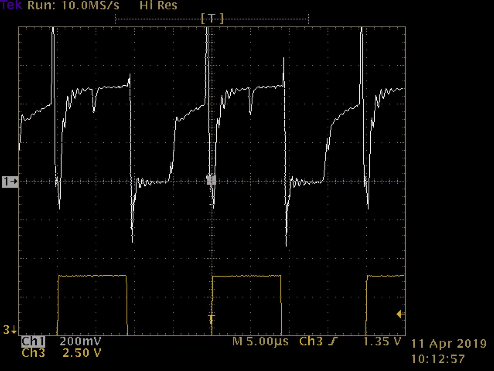
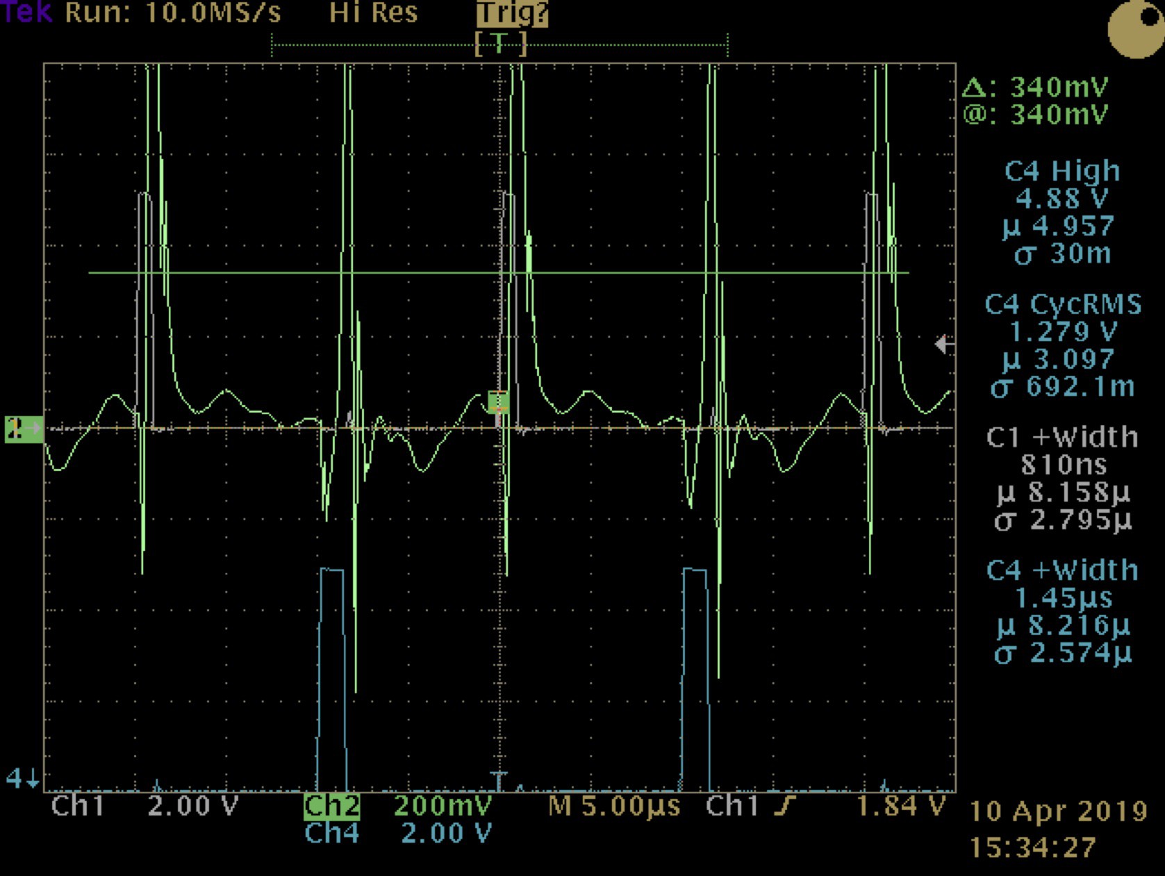
I had a DC blocking capacitor on the AC output in early prototypes but found it unnecessary.  After that I didn't do much investigation on why but I suspect it's similar to the self-balancing effect you get with MOSFETs on the transformer bridge:  an imbalance increases current on that leg of the bridge which raises junction temp, increasing their Rds(on), thereby reducing current.  Somewhat ironic since the output inductors are designed as DC.

I haven't encountered problems running old-school gear.  In fact, the cover photo with the TV has the audio running thru an early 90's Denon receiver/amp that uses a line transformer & linear supply.

  Are you sure? yes | no

Paul Breed wrote 05/14/2019 at 12:50 point

On  a quick read I did not see any discussion on controlling DC bias in the output.
(I was lazy and did not load up the schematics so it might be there)

A modern switching supply load probably does not care, an old school transformer cares a lot. Any tiny DC bias will drive a transformer based load into core saturation.
(IE the offset in a good op-amp will cause saturation issues)

In a previous Job we would monitor the peak current both + and -  and drive the DC bias to make them the same...

This works great for a transformer load, it  has issues with things like single rectifier  low current parasitic supply. Alas most of the world is now a power factor corrected switcher-that would probably run mostly fine on DC. If I remember correctly we limited the authority of the bias correction to  something like 1 V or so to handle the one rectifier case.


  Are you sure? yes | no

Dan Maloney wrote 05/10/2019 at 17:26 point

Wow, super detailed! This is useful stuff - thanks!

  Are you sure? yes | no

Similar Projects

Does this project spark your interest?

Become a member to follow this project and never miss any updates