The TS50 is a Frankenstein unit that is the amalgamation of three separate projects: a DC-DC buck, a DC transformer, and a digital sine wave generator.
Being a power geek, it all began with my nutty interest in inverters - part of my mad scheme to build an ecosystem of off-grid energy management stuff. Specifically, those that output a true sine wave without the use of a boat anchor 60Hz line transformer.
My working concept was a two-stage process: first a DC-DC boost stage followed by a PWM-based sine stage. This was all new for me so considerable R&D was necessary.
First I built a bare-bones full-bridge DC transformer. I named it 'inv48', it's purpose was to boost 12VDC to 48V - multiples of the input voltage but still relatively safe. I needed a platform to learn transformer core types and winding methods, trade-offs, and efficiencies. Anyone that has designed & built transformers knows that designing them on paper is science but, building them is an art.
With this unit I trialed several transformers, mostly RM cores, with powers ranging from 50-100 Watts. Multiple secondaries, both single & center-tapped and with various winding ratios. Interleaved & polyfilar winding methods and their impact on leakage inductance & parasitic capacitance were explored. Eventually the transformer designs exceeded the original 48V target and delivered a clean 170VDC with power delivery well beyond 100W. The project's PCB & current sense machinery now became the limiting factors to what I could do.
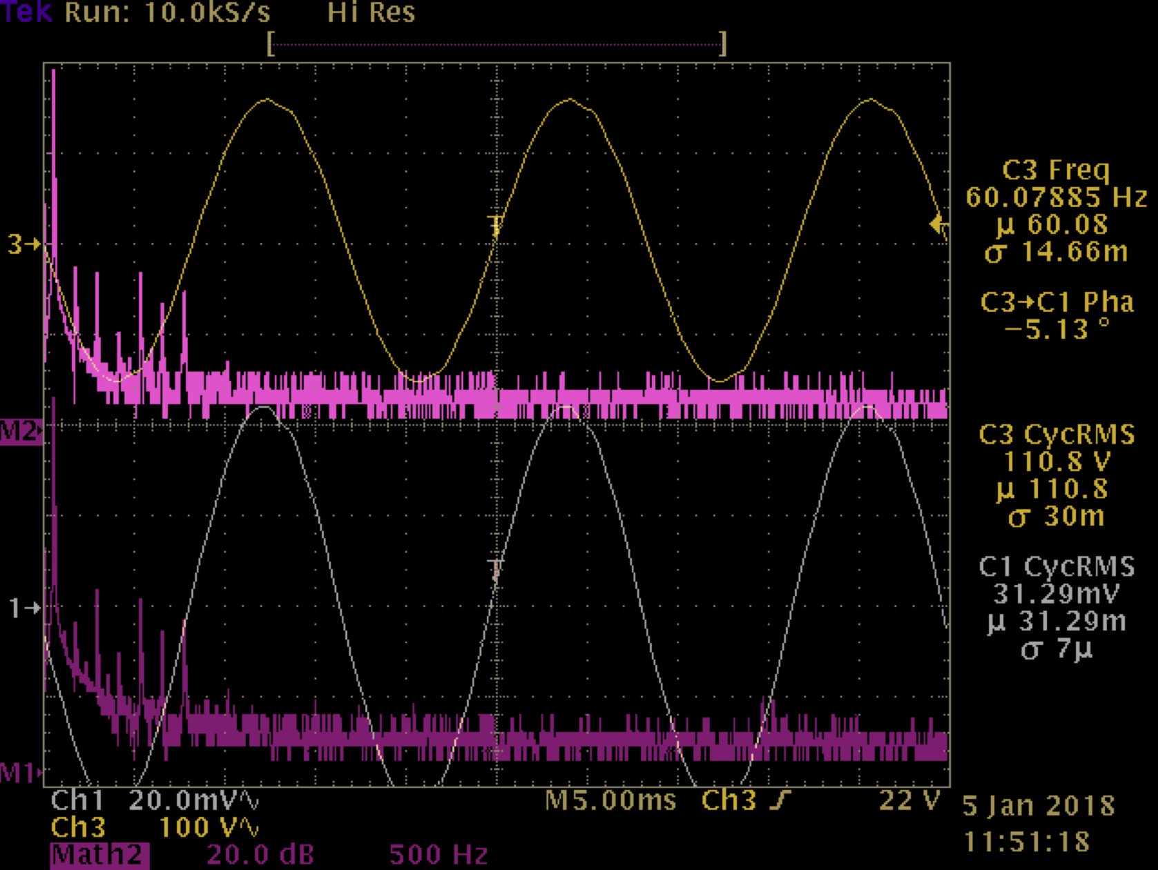
I then moved on to generating a sine wave with a new project PCB. I named it 'sd16f324' - Sine Demo and 16f324 for the PIC MCU I used to generate the PWM signal and control the bridge. Like the inverter, this design employs a full bridge but instead of driving a transformer it's connected to an L-C filter much like a buck; it also functions much like a synchronous buck. The sine wave is generated by applying a PWM signal across the bridge with the duty cycle representing the sine angle. The bridge applies this signal in one direction, building from a DC of 0% @ 0˚ to ~ 99% @ 90˚, decaying to 0% @ 180˚ and, then reversing direction and repeating the cycle.
Like the inverter work, this platform proved very useful and allowed investigation in several areas:
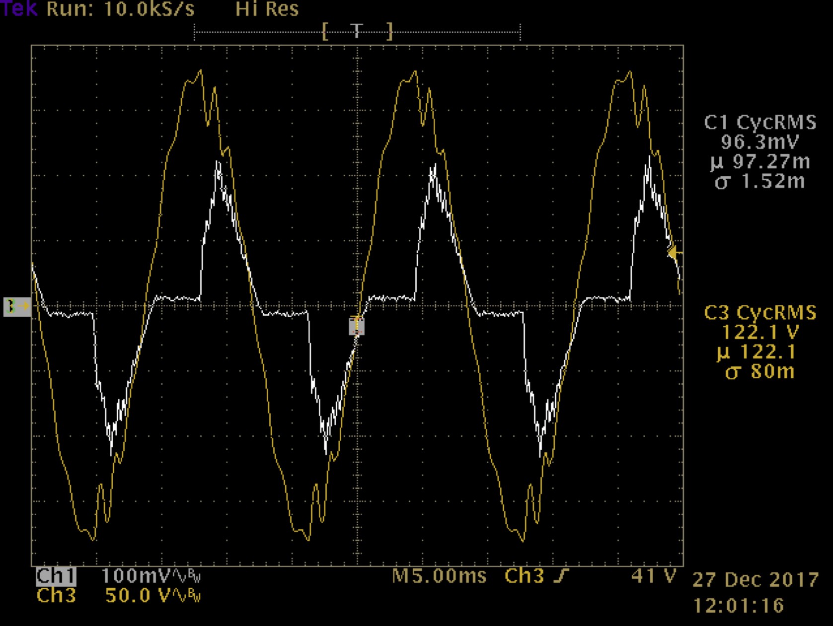
- The effects of resistive & reactive loads
- Inrush current (one of the more challenging areas)
- Distortion & harmonics in the AC current & voltage waveforms
- Variations in PWM frequency, timing and duty cycle
- The effect of higher & lower inductances in the output inductor
As you might guess I used inv48 to drive sd16f324. This too proved very useful in investigating inrush, over-current limiting, and regulation.
Satisfied that I had learned enough to be dangerous I mothballed these projects and started a new one that brings it all together in an integrated design. The TS350 is now underway and is intended to deliver 350W continuous with surge capability to 500W. Eventually I'll post this work too.
It always saddens me to see old work, having served its purpose, abandoned & collecting dust. So while waiting for the TS350's PCB to come back from the fab I got the bright idea to bolt inv48 & sd16f324 together permanently, connect to my 100W solar panel setup in the house, and use it to power the internet connection (cable modem & router/access point) - a whopping 12W.
But there was a problem with this. Some of the components in sd16f324's sine bridge are only rated for 200V (it was intended as an R&D unit) and the DC output from the inverter is 170V with a DC input of 12V. The MPP charger on PV system can drive the battery to ~ 14V and this would be dangerously close to component ratings.
Another mothballed project to the rescue! I had a working prototype of a 12V->5V DC synchronous buck left over from another project. That work...
Read more »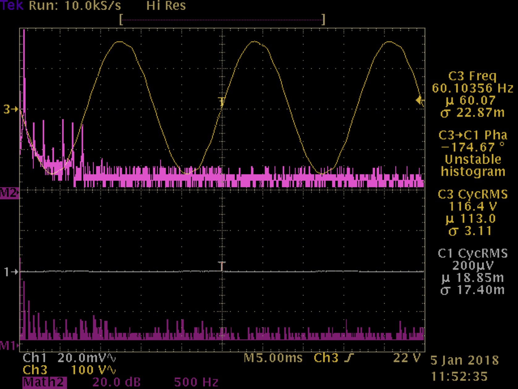


 Evangelos Petrongonas