Hardware modification
I wanted more colorful and better scanning results, so I decided to make some upgrades on the microscope. I needed more flexibility on the alignment setup, and some structural rigidity for less shakiness.
I am not a mechanical engineer and I think everyone see how did it go...
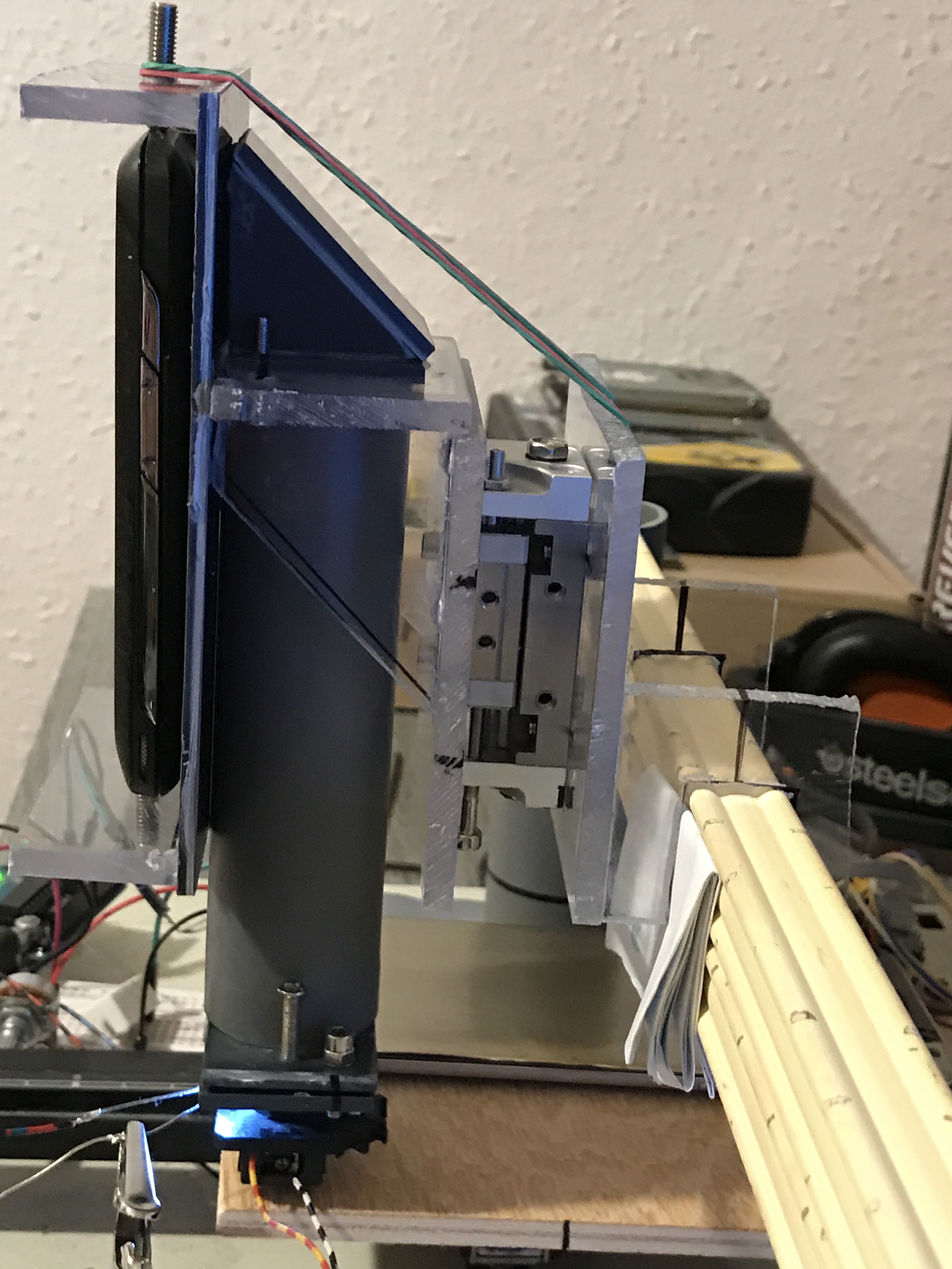
The optical path was much better, I added a leveling option for the CD optical head and a 45 degre mirror to the top to reflect the image to the CCD of an old phone. I had to remove the optic from the front of the CCD in the phone, surprisingly it worked after all. I also added a Z axis mechanicel movement for better hight adjutment.
The resuts was better than before, more details on the images, but I was not happy, because I could not connect the phone to the PC as an USB webcam. The connection is omportant, because if I can not controll the camera from PC, then I am not able to make multiple images and stich them together.
The result is from the Samsung OLED display:
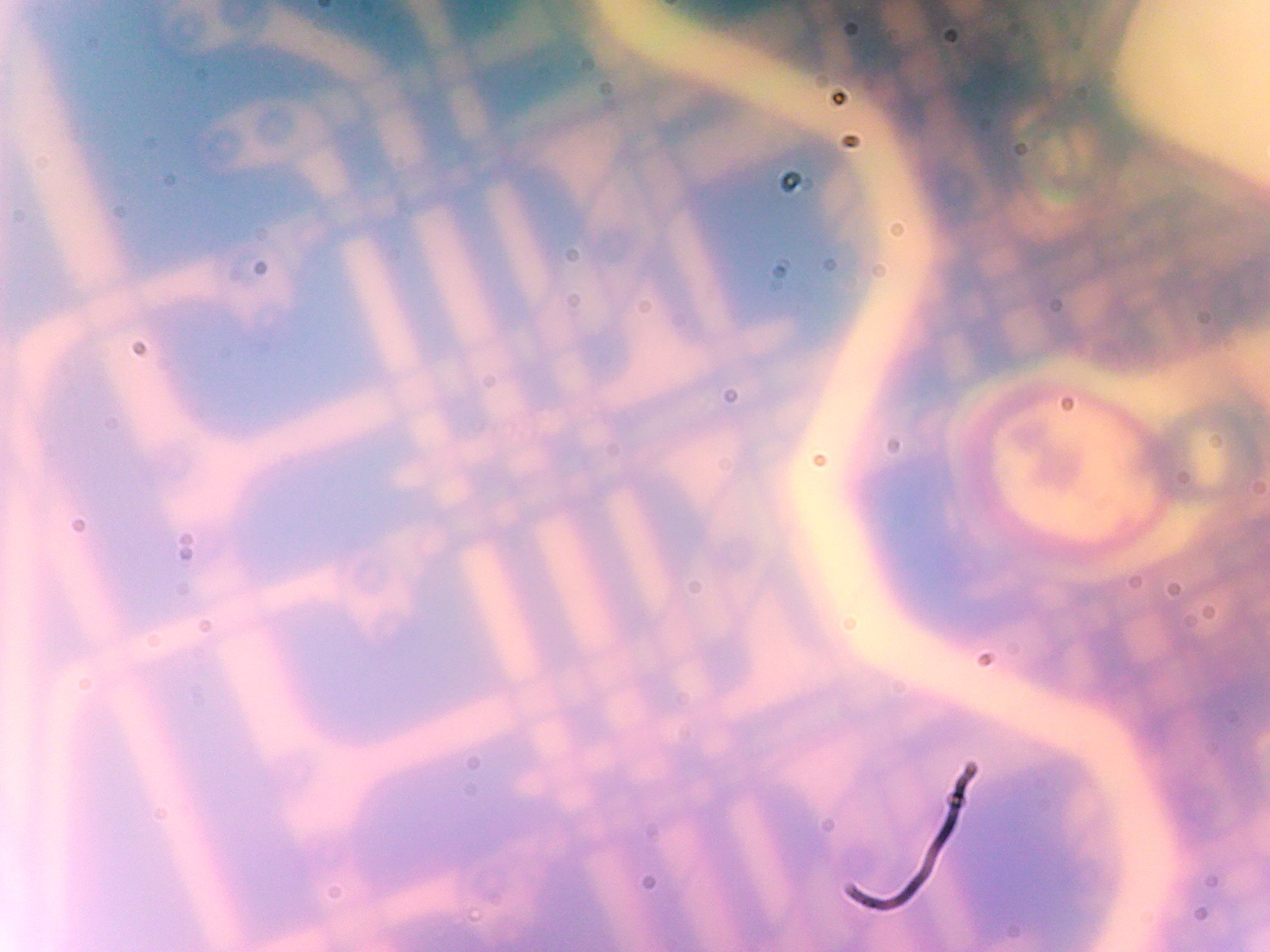
The images was cloudy and the CCD had some particle on it sadly.
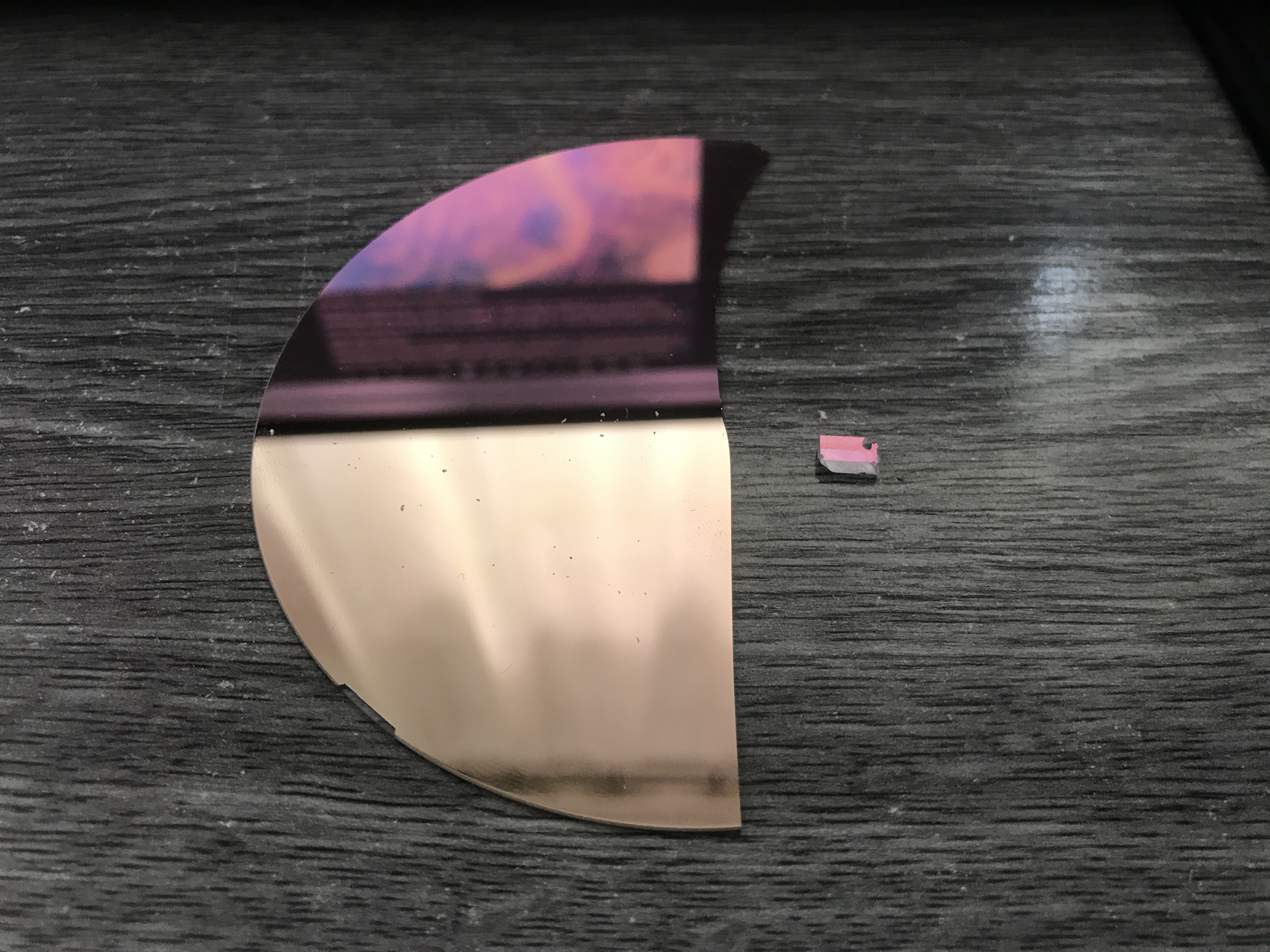
Because of the connectivity problem, I decided to swich the camera back to the USB microscope camera, with some other changes. I wanted to change the beam splitter because it caused a purple6 violet distortion on the images and I lost a lot of other colors because of that beam splitter. I managed to get a sample, who knows what is the layer on it... But it is actualy much better beam splitter then what I had. It has some orage tone, it reflect the light around 590-600nm. The old beam splitter reflected the light more like above 620nm, so it was not for greate for the low visible light spectra.
The new splitter material on the left, the old on the right:
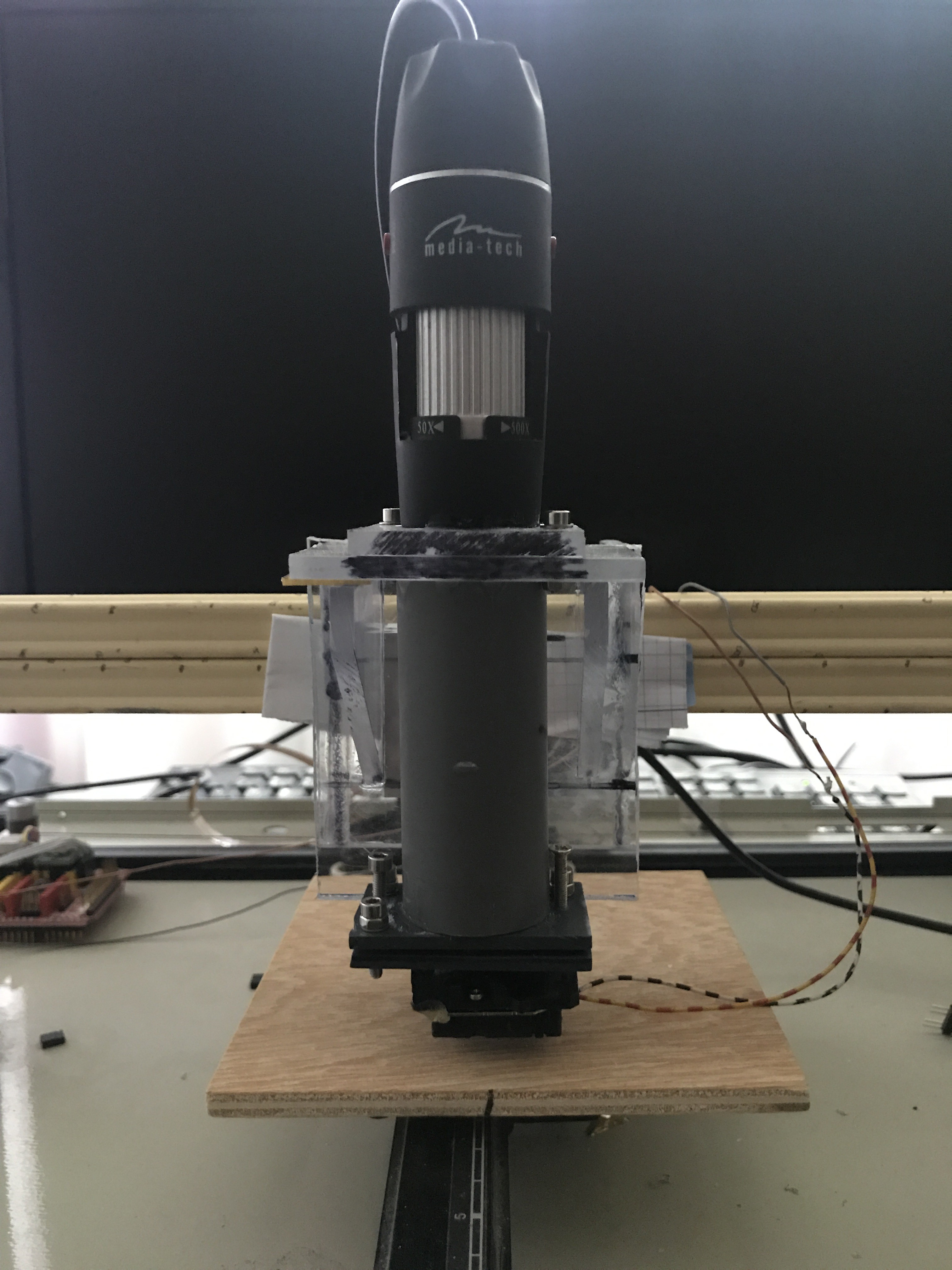
After installing the new beam splitter, I upgraded (downgraded actually) the camera:
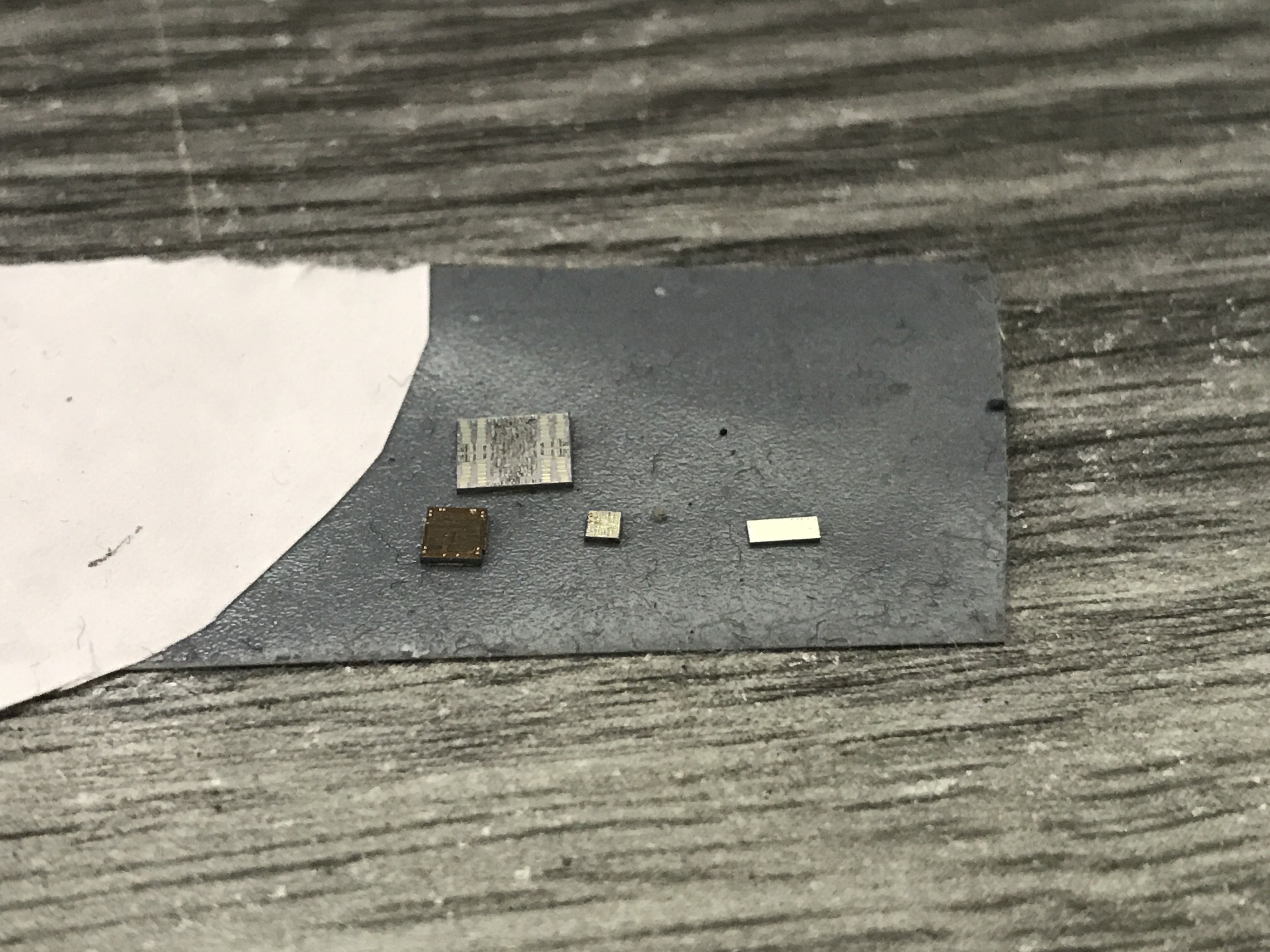
With the more stable optical setup I decided to try scan an integrated circuit. I managed to harvest some bare integrated circuit component, by heating 500 degrees celsius IC packs and cracking the open. AN PIC and some analog IC-s:
These much more interresting than screen circuits. The image quality was insane compared to screen circuits. The mechanical movement of the X-Y stage gave me lot of trouble, because it is not precise enough, and wobble a lot. The image stiching is far from perfect I know, but here is the end result of the first scan:
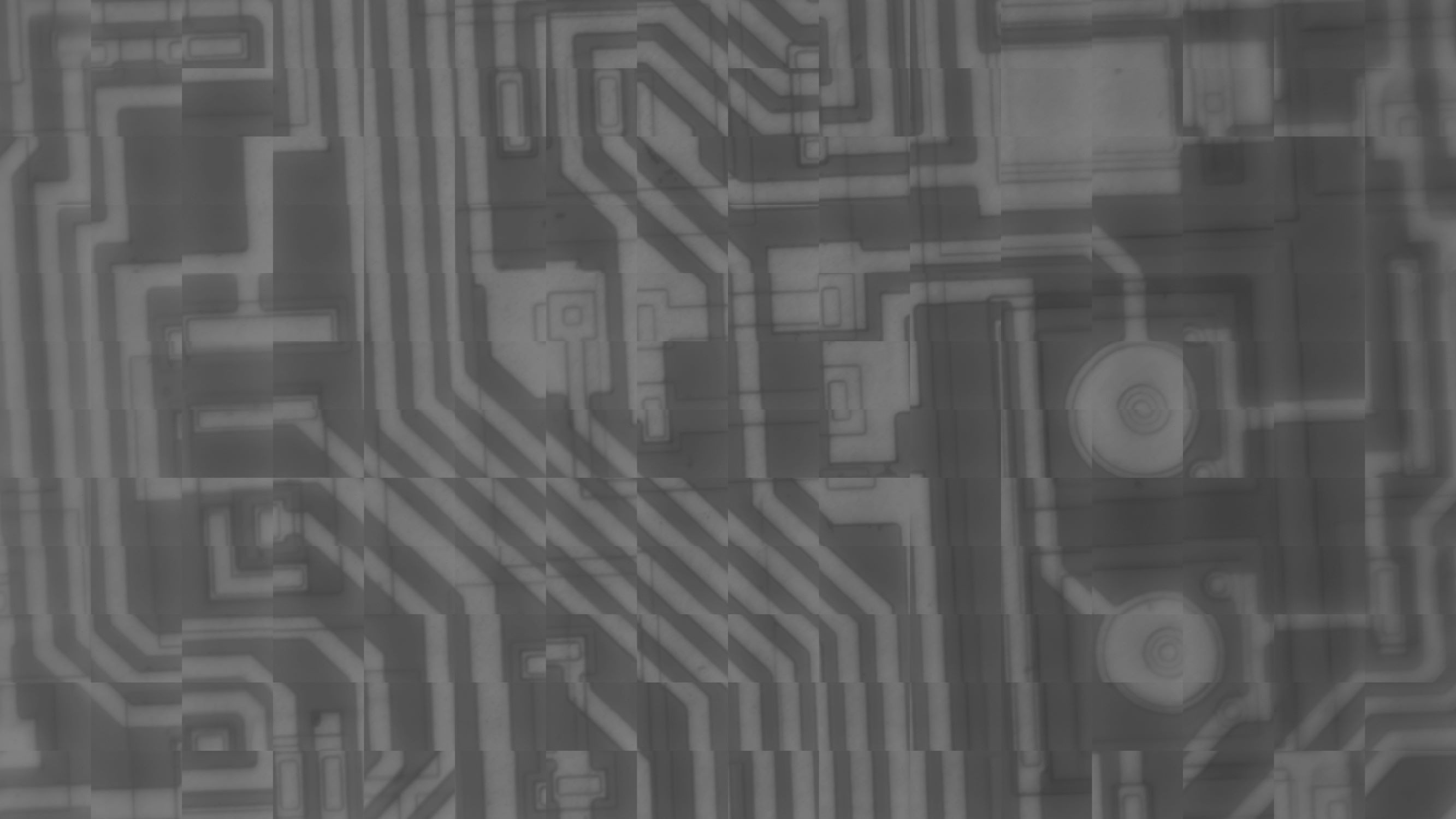
Originaly it is 56,2MP so it is quite large, I had to convet it to 4MP to upload it here.
It is a lot to improve...
My next step is to improve the stiching and get a nice big image, maybe from the full surface area of the IC.
In the future I want to try upgrade it to an Imaging Reflectometer, or make some experience with it at least.
Discussions
Become a Hackaday.io Member
Create an account to leave a comment. Already have an account? Log In.