 Kris Winer
Our STM32L4 line of development boards has been available on Tindie for a couple of years and we have been making good use of the reference designs and Arduino cores for these in custom projects. Some projects, however, require more GPIOs and/or more flash and SRAM memory than the STM32L496 (~50 GPIOs, 1 MByte flash, and 320 kByte SRAM) can provide. Therefore, we decided to take the next step up the value chain and develop a reference design for the STM32L4+ family of MCUs, in particular, the STM32L4S9.
The STM32L4+ family of MCUs generally offers more GPIOs than the L4 family; the LQFP-100 L4+ package offers the fewest but the size of this package is 14 mm x 14 mm, which means more like a ~17 mm x 17 mm footprint on the pcb. This is a bit too big for most of our custom applications. The 0.5-mm-pitch BGA-132 or BGA-169 packages are much smaller but these would require more than 4 pcb layers or more expensive via-in-pad fab methods in order to expose all of the GPIOs to the user. The goal was to develop a reference design that anyone could inexpensively reproduce. In this case, only the 10 mm x 10 mm, 0.8-mm-pitch BGA-144 package meets the small size, easy-to-fab criteria. Such a package allows a design that exposes all of the GPIOs to the user while also allowing use of inexpensive (OSH Park) 4-layer pcb fab methods.
This doesn't mean that the design was easy, and routing was somewhat of a nightmare given the constraint of the 0.7 x 1.4 inch development board form factor.
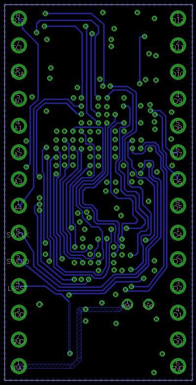
Trace routing on the second pcb layer
We had to use 5-mil trace widths for all of the signal traces in order for them to fit within the area and layer constraints. Still, we managed to make all of the required connections to the external SRAM (~40 connections) and QSPI flash (6 connections) as well as exposing 21 GPIOs at the edge of the board. We exposed Arduino digital pins D0 - 13, SDA/SCL (technically, D14 and 15), and analog pins A0 - A4, nRST, SWDIO, SWCLK for ST LINK V2 programming (if desired), as well as GND, VIN, and 3V3 out. We included a USB connector for easy programming with the Arduino IDE, a 500 nA Iq NCV8170AMX330 3V3, 150 mA LDO, a dual FET for battery voltage monitoring using two GPIOs dedicated for this task, and an RGB led controlled by three GPIOs. So not all of the GPIOs are available for the user in this development board but enough to test the performance of the main STM32L4S9 peripherals and the external QSPI flash and SRAM, which is the main goal for this project.
For the QSPI flash, we chose the same Macronix MX25L12835FZNI 16 MByte NOR flash we use in our Dragonfly L4 development board. The challenge here is making this work with the L4+ OCTOSPI peripheral which is different from the L4 Quad SPI peripheral. In fact, the L4+ has two OCTOSPI peripherals so, in principle, one could have two separate QSPI NOR flash components on the board, or one NOR and one NAND flash, or one flash and one SRAM even.
The issue for SRAM in our application is access speed, meaning speed of writing data and reading data. The OCTOSPI peripheral is likely fast enough and allows for internal memory mapping (in other words, acting like internal SRAM) but one or more errata (problems in L4+ silicon) prevents this from working optimally. So we have chosen to make use of the other memory management peripheral available on the L4+, the FMC.
The Flexible Memory Controller (FMC) provides an interface for statically memory-mapped devices like SRAM, supports 16-bit bus widths, and runs at half the speed of the system clock, up to 60 MHz. So for read/write operations, speed is going to be dependent on the properties of the individual SRAM IC. We have chosen two to evaluate: Cypress CY62167EV30LL-45BVXIT 2 MByte SRAM and ISSI IS65WV102416EBLL-55BLA3 2 MByte SRAM. There is a tradeoff between access speed and power usage (also cost and availability-we wanted to test the FBLL version of the ISSI SRAM but it wasn't available).
We would like to maintain...
Read more »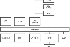
 Kevin Neubauer
 James Cannan
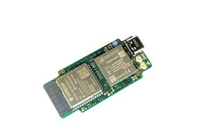
 Daan Pape
Where can i buy the board with the stm32l4s9 chip