0%
0%
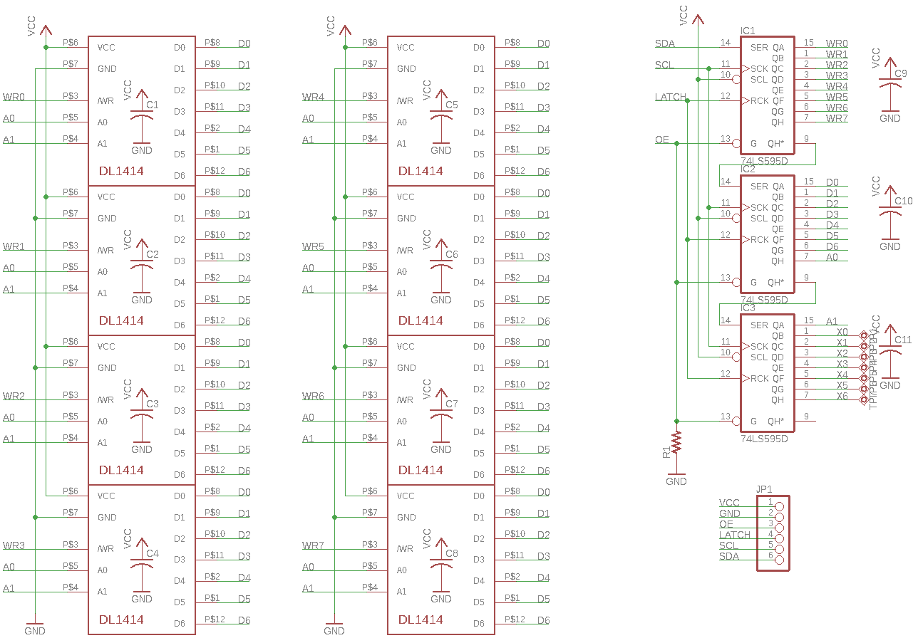
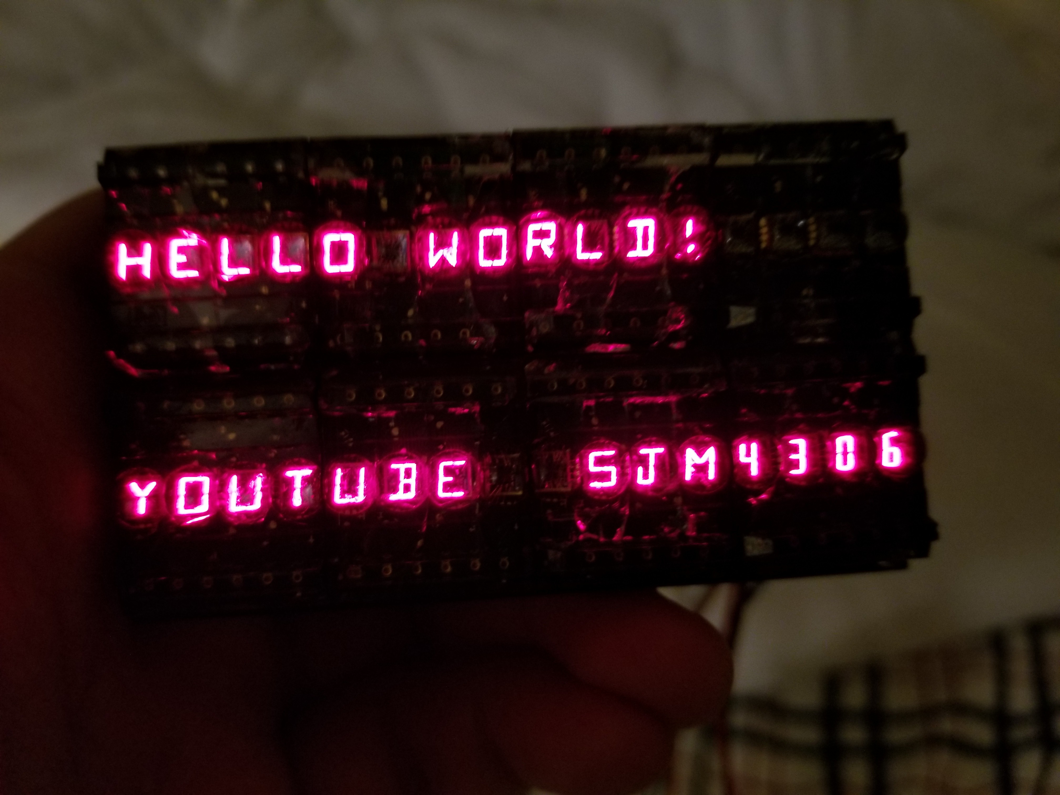
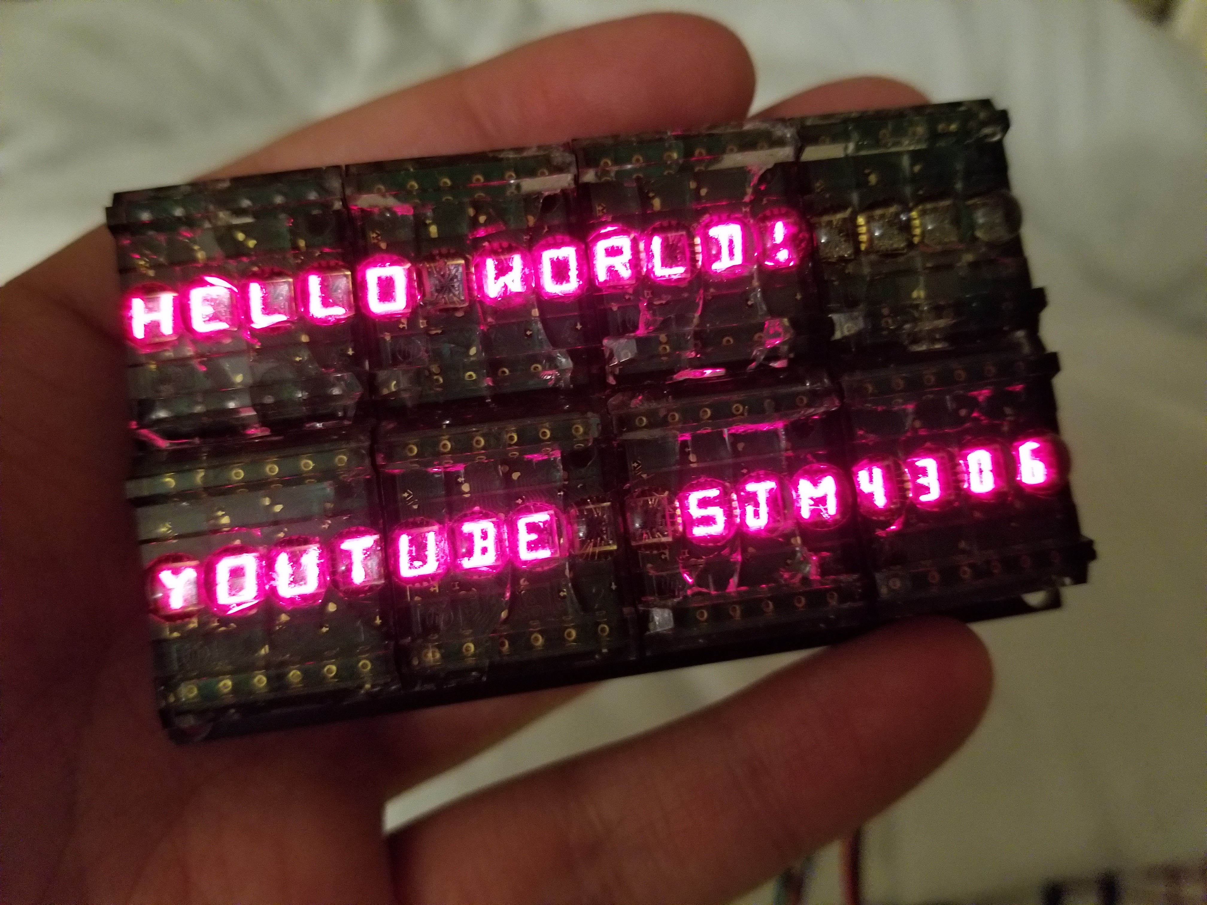
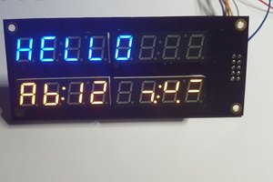
HPDL-1414 16x2 LED Display
I found these cute little retro 4 digit LED displays for less than $1 each so I just had to design a larger serially controlled display.
 sjm4306
Become a Hackaday.io member
Already have an account? Log in.
Just one more thing
To make the experience fit your profile, pick a username and tell us what interests you.
Pick an awesome username
hackaday.io/
Your profile's URL: hackaday.io/username. Max 25 alphanumeric characters.
Pick a few interests
Projects that share your interests
People that share your interests


 Bharbour
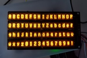
 Matt Stock
Can you provide all the files jlcpcb needs these days order this assembled? Also is it possible to have individial modules for single displays?