 Tim Ryan
TOM-1 is a TTL-based processor with a small instruction set. The idea came from reading about projects like Gigatron and Ben Eater's 8-bit video series, as well as Verilog CPU implementations like nybbleForth. The design goal is to minimize chip count while still offering a 16-bit data bus and being useful for computation.
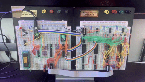
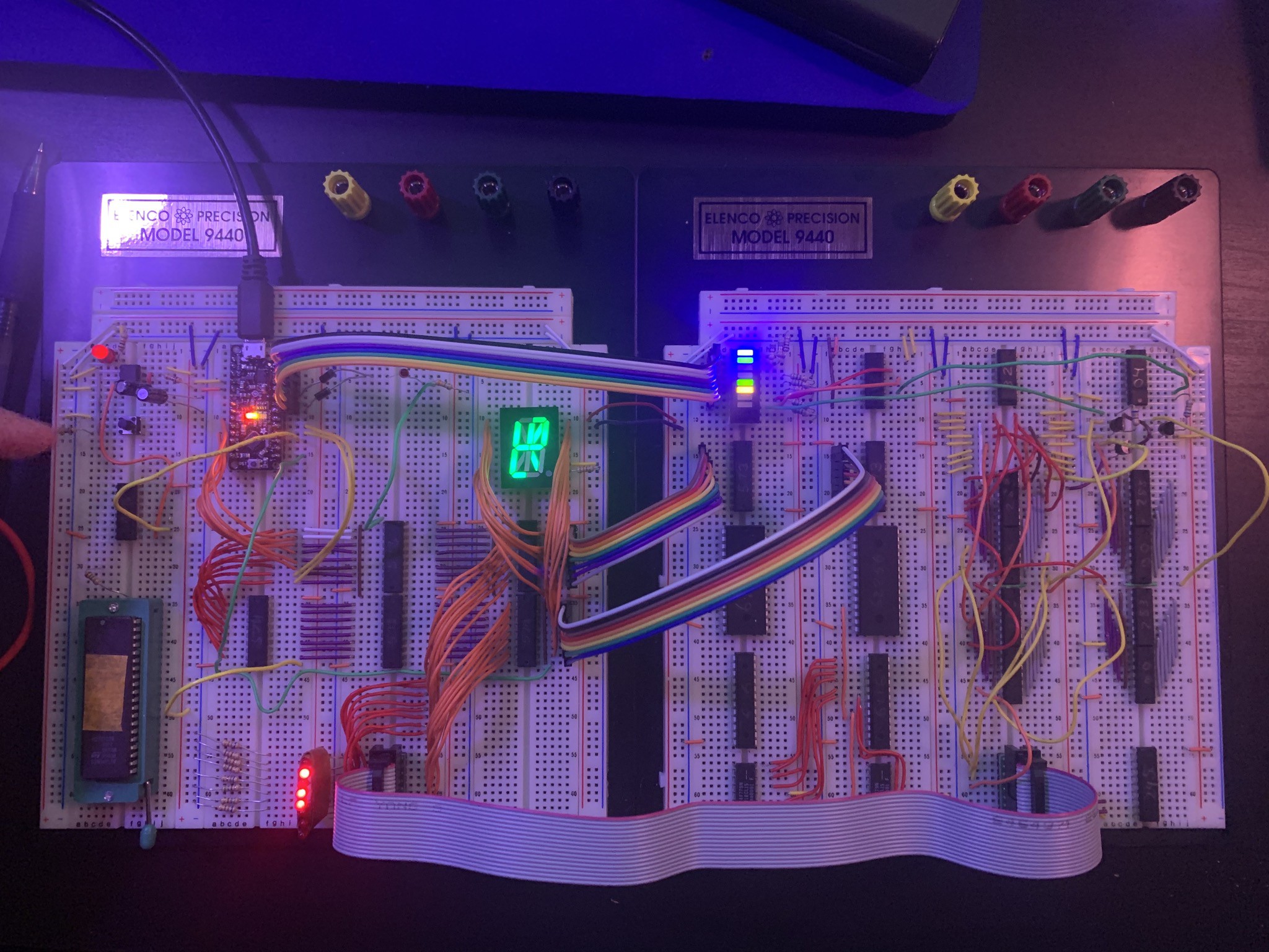
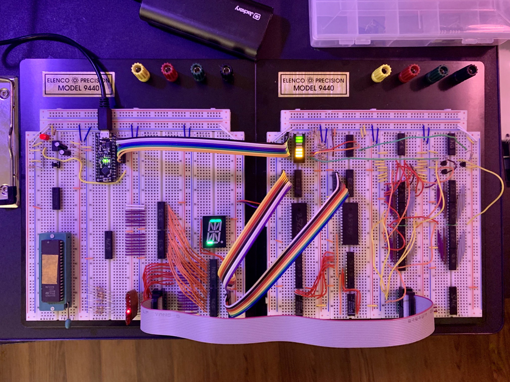
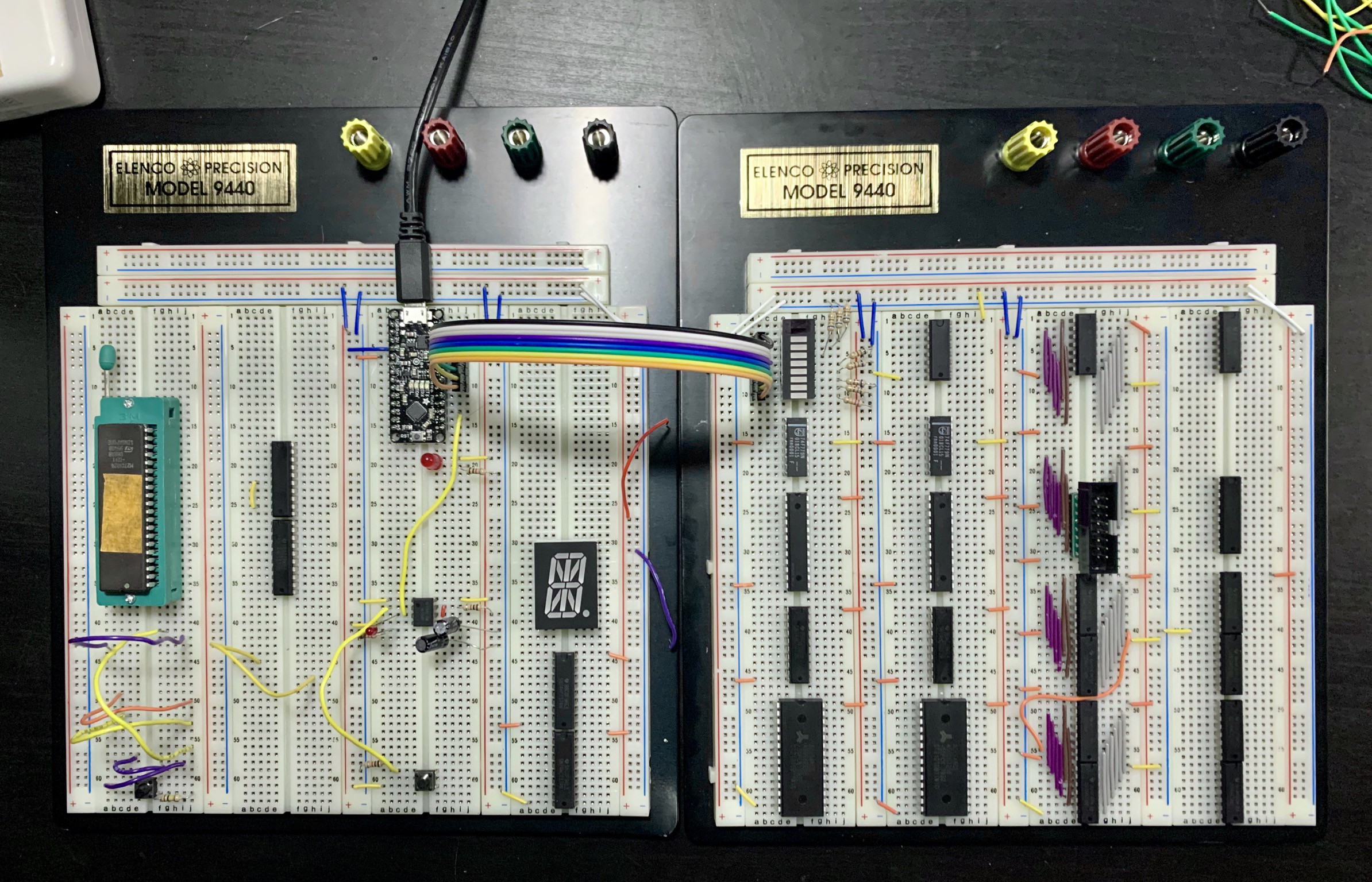
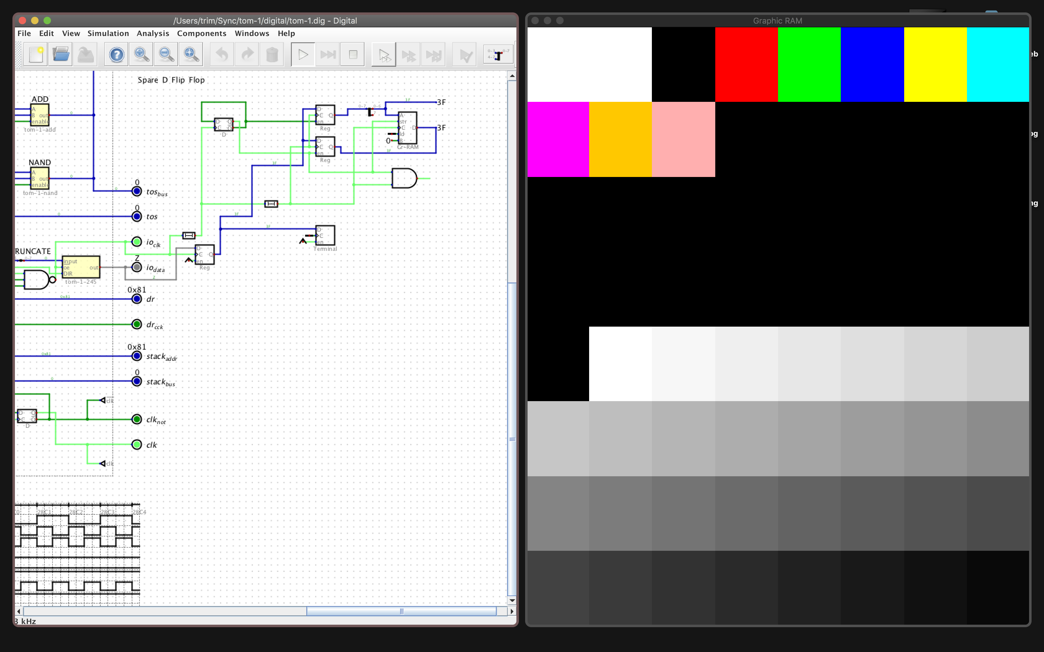
Status: The CPU has been modeled in Digital and the circuit is available on Github. I'm now building the CPU on a breadboard.
Overview
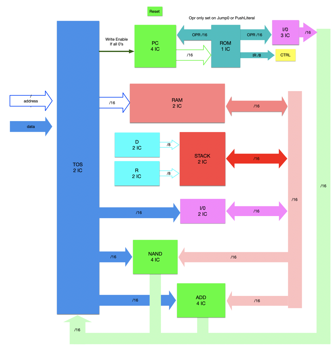
- 16-bit data bus and address space
- Stack machine with separate data and return stacks
- Supports two 16-bit ALU operations (NAND and ADD)
- Not microcoded
- Harvard architecture (ROM and RAM do not share address space)
- CPU can be built using 24 7400-series chips, 4 RAMs, and 1 ROM
Here is a system diagram of the TOM-1 (click for full size):
Addressing
TOM-1 performs one 4-byte operation every two clock cycles. This includes two control bytes and a 16-bit operand, though we interleave how these values are written. Because the final design will use a 27C1024, which has a 16-bit data bus, we dedicate the low byte to a 16-bit operand and the high byte to processor control flags:
PUSH_LITERAL(0x4299) encoded in ROM:
   0000:         1c42
   0001:         0c99
   0002:         ....
In this binary, 0x1c and 0x0c control on each clock cycle how values are loaded into the top of the stack and how values are pushed onto the data stack. As for the lower byte, the circuit uses a latch on every other clock cycle so it can can access both bytes of this two-byte operand at once (0x4299). The top of stack register (TOS) is written at the end of the opcode when all 16-bit values are available.
Opcodes
This is a non-exhaustive list of opcodes supported by the TOM-1:
- halt
- no_op
- push_literal — pushes a 16-bit operand to the top of stack
- branch0 — if the top of stack is equal to 0, jump to a 16-bit address (operand)
- add — pops values A and B from the data stack, pushes the value A + B to the top of stack
- nand — pops values A and B from the data stack, pushes the value A nand B to the top of stack
- load — pops an address from the stack, pushes the value of that address in RAM to the top of stack
- store — pops an address, then a value, from the stack and sets that address in RAM to the value
- return_push — pushes the value at the top of the stack onto the return stack
- return_pop — pops a value off the return stack and pushes it to the top of stack
- dup — duplicates the value a the top of stack
- drop — drops the top of the stack
- in — read a value from the 8-bit I/O port
- out — output a value on the 8-bit I/O port
I/O Port
The I/O port on the TOM-1 is a bidirectional transceiver that can read and write to any address in RAM. This port has the following pins:
- Power
- GND
- 8 bits of data (low byte of 2-byte value in RAM)
- CLK
- Data Valid
Because the bus can only send or receive 8 bits each clock cycle, and the CPU does not support interrupts, this port is best suited for CPU-driven protocols like parallel clocked output or SPI. The port is also not latched, so external circuitry must respect the "Data Valid" bit, and latch on the rising edge of CLK while this bit is high.

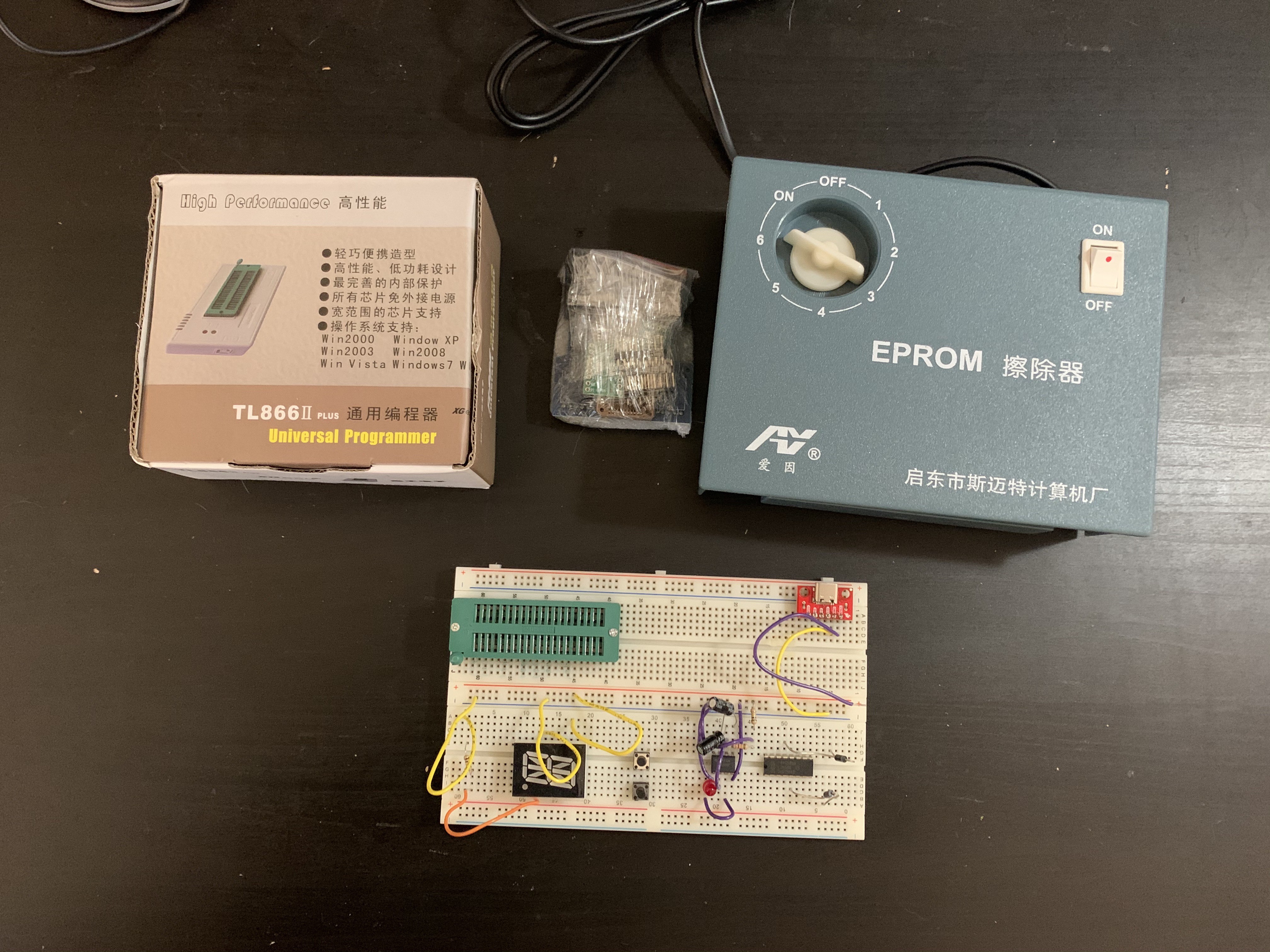 Having done as much as I can for the moment in Digital, it's time to switch over to validating in circuity. I bought an EPROM programmer and UV eraser online for the M27C1024, a 256x16 bit EPROM that this is now obsolete, but which has the rare property of having a 16-bit wide data bus. Getting one of these EPROMs will probably take another week or two.
 ammarbhayat28
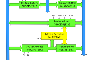
 zpekic
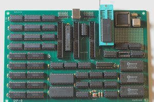
 kaimac