Timo
Timo-
I'm on vacation
09/05/2014 at 20:28 • 0 commentsI did not advance to the next round, so I've got time to go on vacation. ^^
Work will continue later.
-
Raspberry Pi Connection
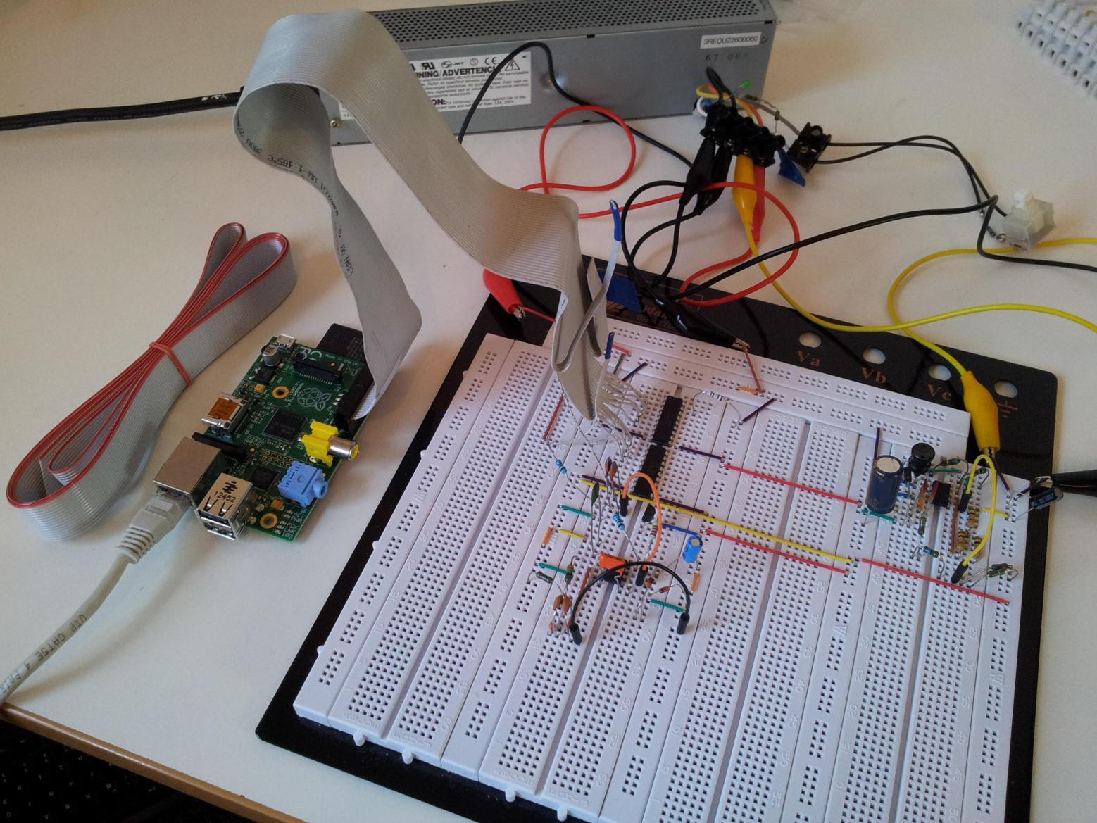
08/20/2014 at 14:15 • 0 commentsI connected the RasPi with an old floppy IDE cable (cut at one end). It has 8 more pins than the Raspberry Pi, so these are ignored (would be cable ids 27-34).
![]()
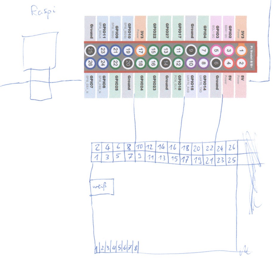
Here is the mapping of RasPi pins to floppy cable ids (only the first 26 of 34 can have a connection):
![]()
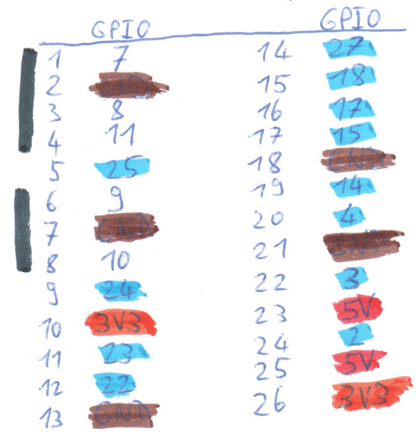
Mapping as seen from the cable (7 pins have a cable connection, but aren't used on the board (the black ones)):
![]()
Color coding:
Black: Not connected
Brown: Ground
Red: 5V
Orange: 3.3V
Blue: Used GPIO Pins
The two 5V pins are connected to the breadboards 5V lane, so it is powered through the board. The two 3.3V lanes are used in the 555 timer circuit from one project log ago. Three ground lanes are connected to the ground of the breadboard and two ground lanes aren't connected.
GPIO25 (cable no. 5 between the black blocks) is used for triggering the 555. All other eleven GPIOs are connected to one port of an ULN2803A chip (the long chips in the top) each.
For connectivity I'm using the LAN cable seen in the picture, later I will add a WiFi or Bluetooth dongle.
-
Prepare for Raspberry Pi interaction
08/20/2014 at 13:10 • 0 commentsThe Raspberry Pi can't guarantee the timing on its GPIO pins due to multi-tasking.
So I need to assure a maximum on-time of the inkjet cartridge nozzles in hardware.
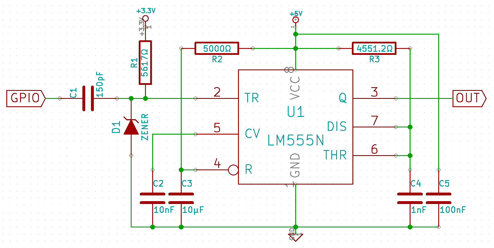
I'm using a 555 in monostable mode for this task: SA555P from TIhttp://datasheet.octopart.com/SA555P-Texas-Instruments-datasheet-7285002.pdf
One obstacle is the fact that a TRIG signal overrides a THRESH signal.
Which means I need to shorten the pulse in order to shorten the pulse ...
But there's hope: Using an RC-filter at the GPIO roughly shortens the pulse, for fine-tuning and sharp edge is the 555 responsible.
Circuit diagram (calculations below):![]()
RC-trigger part (C1, R1, D1):
D1 is a Zener diode of 3.6V protecting against overvoltage. The datasheet tells, that the trigger pin of the 555 gives max. 2µA at 0V. In order to trigger the 555 the voltage needs to stay below 1.1V, so let's say: The capacitor C1 must take at least 300ns (some time off the datasheet) to reach the level of 1V through resistor R1. To deal with 2µA, let's see that the maximal flow is much bigger than 2µA (= ignore this amount).
Starting with some ballpark values:
1mA maximal flow gives
1mA => 3.3V / 1mA = 3300Ω =: R1
Give it 300ns to rise up to 1V (buffer of 0.1V included):
Uc = Umax * (1 - e^(-t / (R * C)))
1V = 3.3V * (1 - e^(-300ns / (R1 * C1)))
<=> e^(-300ns / (R1 * C1)) = 1 - 1V / 3.3V
<=> -300ns / (R1 * C1) = ln(1 - 1V / 3.3V)
<=> C1 = -300ns / (R1 * ln(1 - 1V / 3.3V))
So R1 = 3300Ω => C1 = 251.82pF
I got an R1 with 5617Ω which sets C1 = 147.94pF.
My C1 got a measured capacity of 180pF.
Capacitor C2 is just for stabilization. Most circuits I've seen used 10nF, I had 22nF lying around.
Reset time: R2 + C3
This gives some time till the chip has functionality, so it doesn't start with a peak at OUT.
Again doing some ballpark calculations: Say 10µs as a start and charging with 1mA, so worst case RESET current is dealt with. The voltage level must be held below 0.3V in that time.
Uc = Umax * (1 - e^(-t / (R * C)))
0.3V = 5V * (1 - e^(-10µs / (R * C)))
<=> 0.06 = 1 - e^(-10µs / (R * C))
<=> e^(-10µs / (R * C)) = 0.94
<=> -10µs / (R * C) = ln(0.94)
<=> R * C = -10µs / ln(0.94) = 0.0001616151s
C := 10nF => R = 16161.510712Ω
C := 100nF => R = 1616.1510712Ω
Maximal flow:
5V = R * 1mA => R = 5kΩ
=> C = -t / ln(0.94) / 5kΩ
C = t * 0.0032323 / Ω
309.377µs per µF, thus using some µF capacitor.
Result: Using R2 around 5.5kΩ and C1 with 22µF, but the exact values doesn't matter that much, just deactivating the chip for a few ms.
Set the 555 pulsetime through R3 and C4:
pulsetime = ln(3) * R3 * C4
(Most circuit calculators use 1.1 instead of ln(3), because ln(3) = 1.09861228867.)
I want a pulsetime of 5µs, so:
5µs = ln(3) * R3 * C4
Take a look at some test values:
C4 := 10nF => R3 = 5µs / ln(3) / 10nF = 455.1196Ω
5V = 455.1196Ω * I => I = 0.01098612A (while discharging)
11mA is a bit too much for standby in my opinion.
Since things are linear in this formula, let's divide it by 10.
New try
C4 := 1nF => R3 = 5µs / ln(3) / 1nF = 4551.196Ω
5V = 4551.196Ω * I => I = 0.001098612A (while discharging)
1.1mA is better and fine, because it is lower than the typical current consumption of the chip itself (3mA).
I got R3 with 4570.4Ω and C4 with 1nF.![]()
-
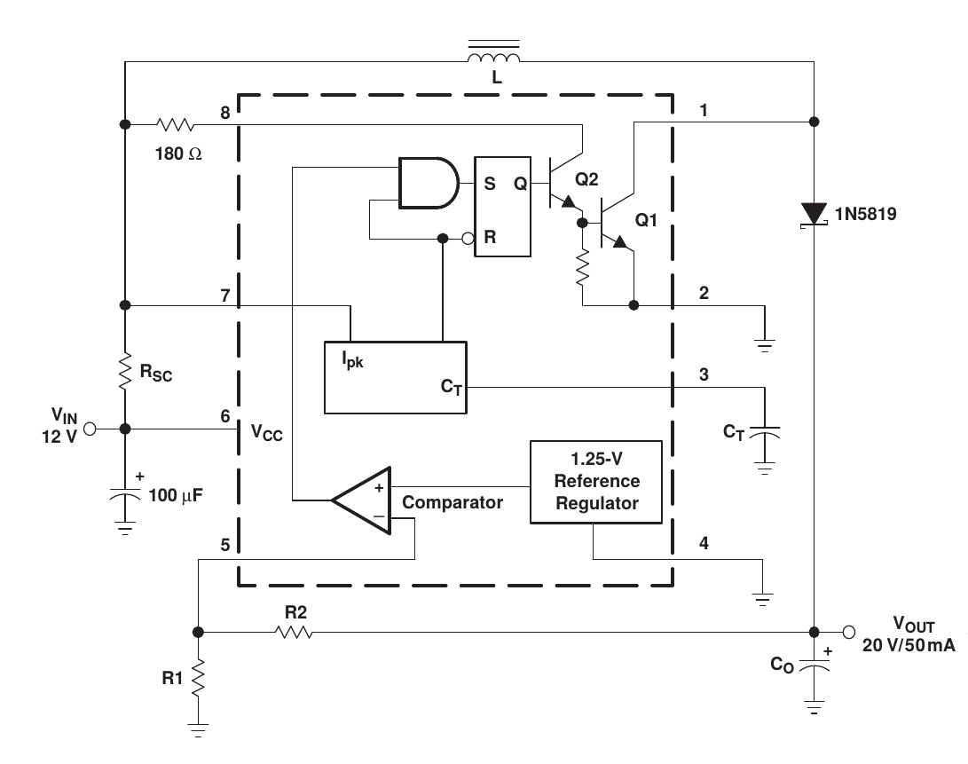
DC-DC Step-Up Converter
07/30/2014 at 19:35 • 0 commentsI will need 20V for one of the ink cartridges (HP C6602A). So I need to step up my voltage from 12V to 20V. Here I use a step-up dc-dc converter around MC34063 (from UTC in this case).
Multiple datasheets for MC34063 are available, e.g.:
http://www.onsemi.com/pub/Collateral/MC34063A-D.PDF
http://www.ti.com/lit/ds/symlink/mc33063a.pdf
Even some in depth discussion:
http://www.onsemi.com/pub_link/Collateral/AN920-D.PDF
http://www.ti.com/lit/an/slva252b/slva252b.pdf
Calculators and diagrams:
http://dics.voicecontrol.ro/tutorials/mc34063/
http://www.nomad.ee/micros/mc34063a/
Video-tutorial by David L. Jones (funny and informative):
http://www.eevblog.com/2010/09/10/eevblog-110-lets-design-a-dc-to-dc-switchmode-converter/Diagram with missing values (calculated below):
![]()
Here are my calculating steps for the missing parts. The following parameters are chosen initially:
Vin = 12V - 10% = 10.8V (10% safety margin)
Vout = 20V (needed for one of the ink cartridges)
Vf = 0.4V (forward dropping voltage of diode by datasheet)
Vsat = 0.5V (switch saturation voltage by datasheet)
f = 100kHz (maximum frequency)
Iout = 50mA (starting low, have to see, what's really needed)
Begin with calculations (just plug in values one-by-one):
ton/toff = (Vout + Vf - Vin) / (Vin - Vsat) = 0.9320388
ton+toff = 1/f = 10µs
toff = (ton + toff) / (ton / toff + 1) = 5.17588µs
ton = (ton + toff) - toff = 4.82412µs
Ct = 4 * 10^(-5) * ton = 193pF (used 2 * 82pF measured as 200pF)
Ipk = 2 * Iout * (ton/toff + 1) = 0.1932A
Rsc = 0.3 / Ipk = 1.55Ω (1Ω in series to 2 * 1Ω in parallel = 1.5Ω)
Lmin = (Vin - Vsat) / Ipk * ton = 257µH (used 330µH)
Instead of choosing Vripple, I used a 470µF low ESR cap and therefore (this part of) the ripple is very low.
Co = 9 * Iout * ton / Vripple (used 470µF, so this part of the ripple is 4.6188mV)
Vout = 1.25 * (1 + R2 / R1)
=> (Vout / 1.25 - 1) * R1 = R2
here: 15 * R1 = R2
From AN920-D.PDF (see links above): The current through R1 + R2 shall be 500µA.
=> R1 + R2 = 16 * R1 = 20V / 500µA
=> R1 = 2.5kΩ => R2 = 37.5kΩ
I don't have those values, so I use (measured values):
R1 = 2386Ω (5473Ω and 4230Ω in parallel)
R2 = 35820Ω (976Ω and 34844Ω in series)
R2 / R1 = 15.0126 (quite good value)
The driver collector got 123.9Ω + 61.8Ω = 185.7Ω.The input filter capacitor is a 100µF/16V low ESR cap.
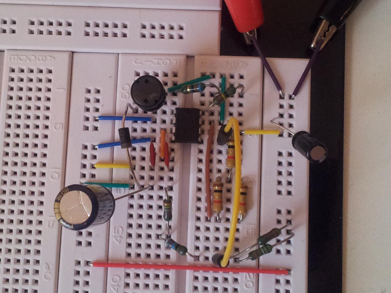
Finished circuit:
![]()
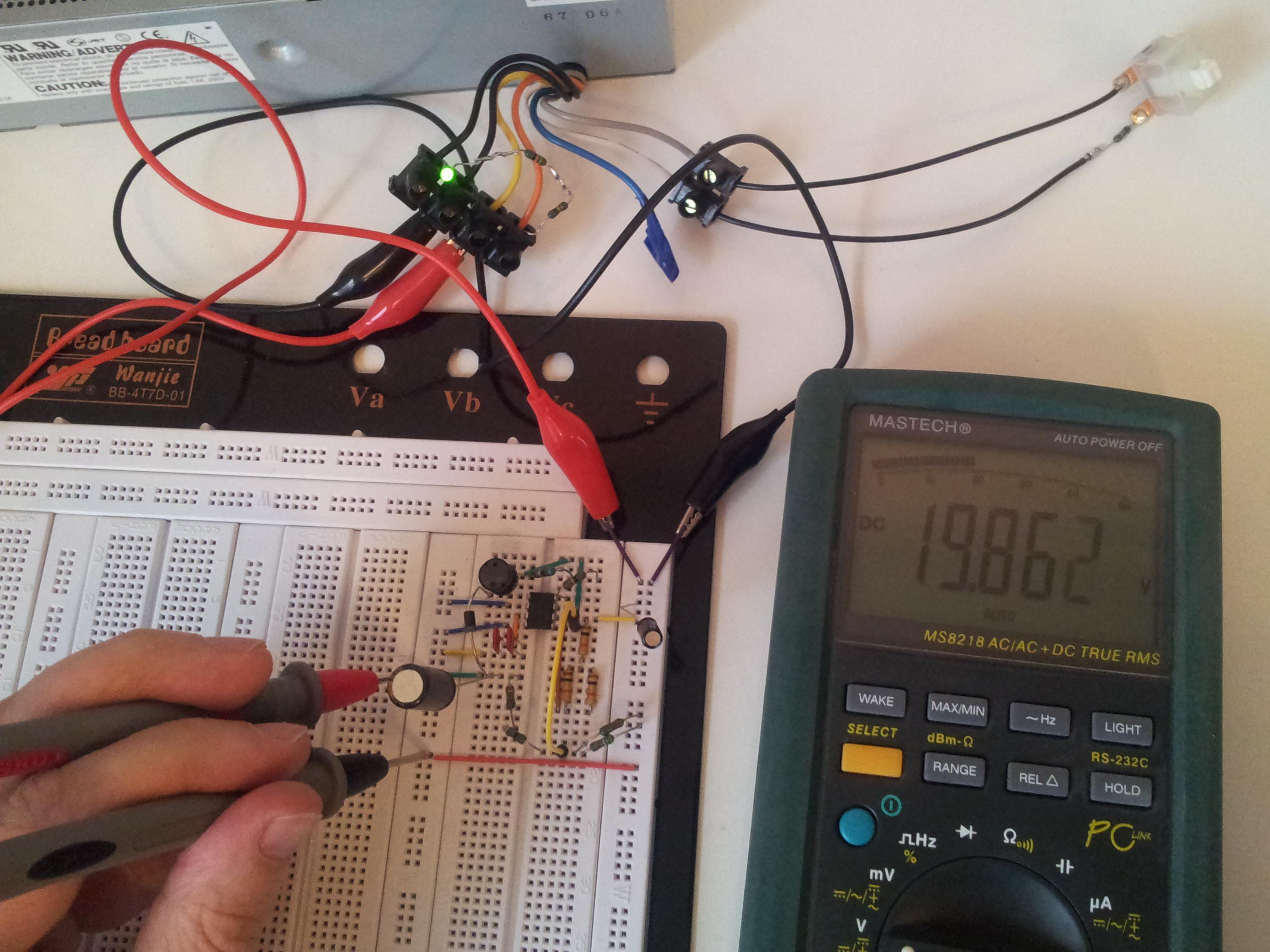
Measuring:
![]()
-
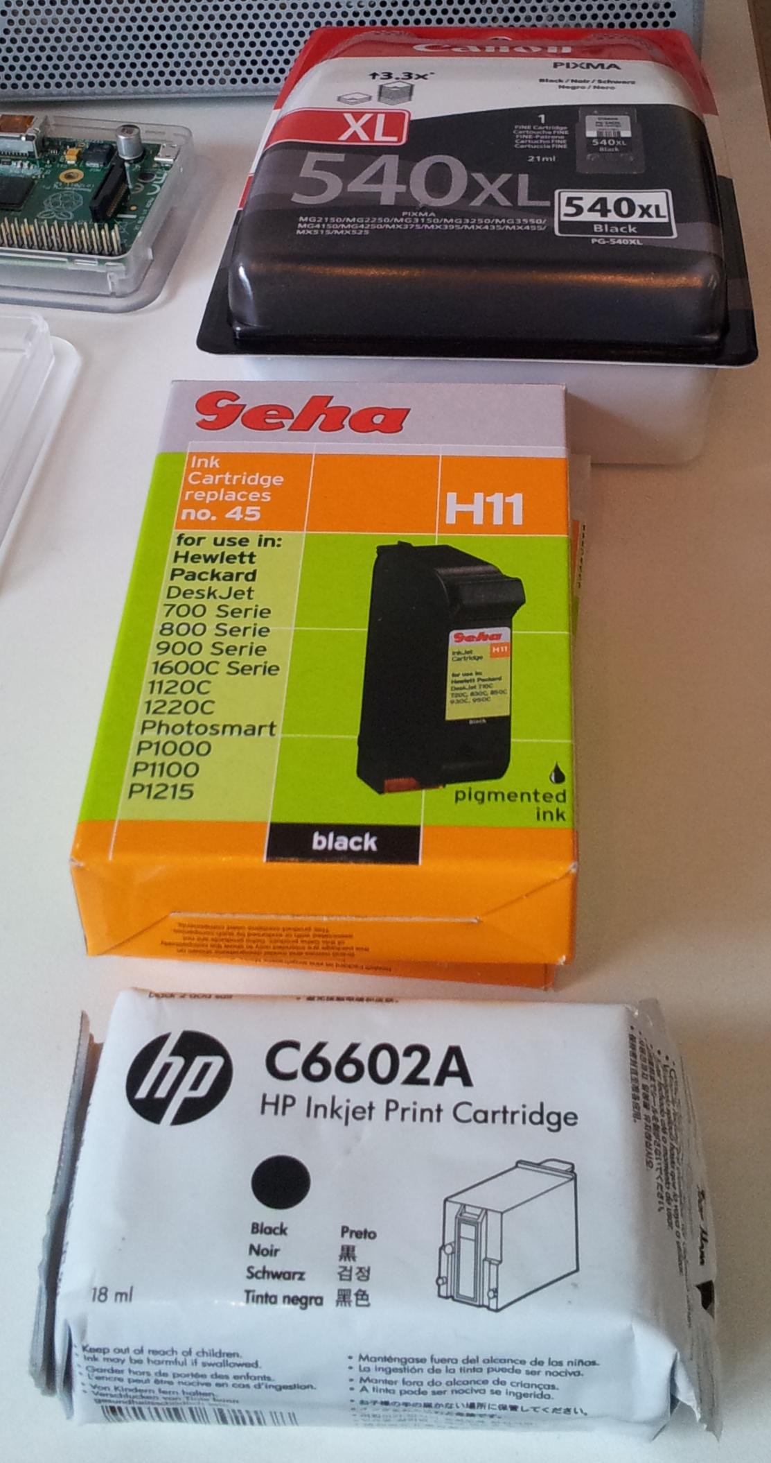
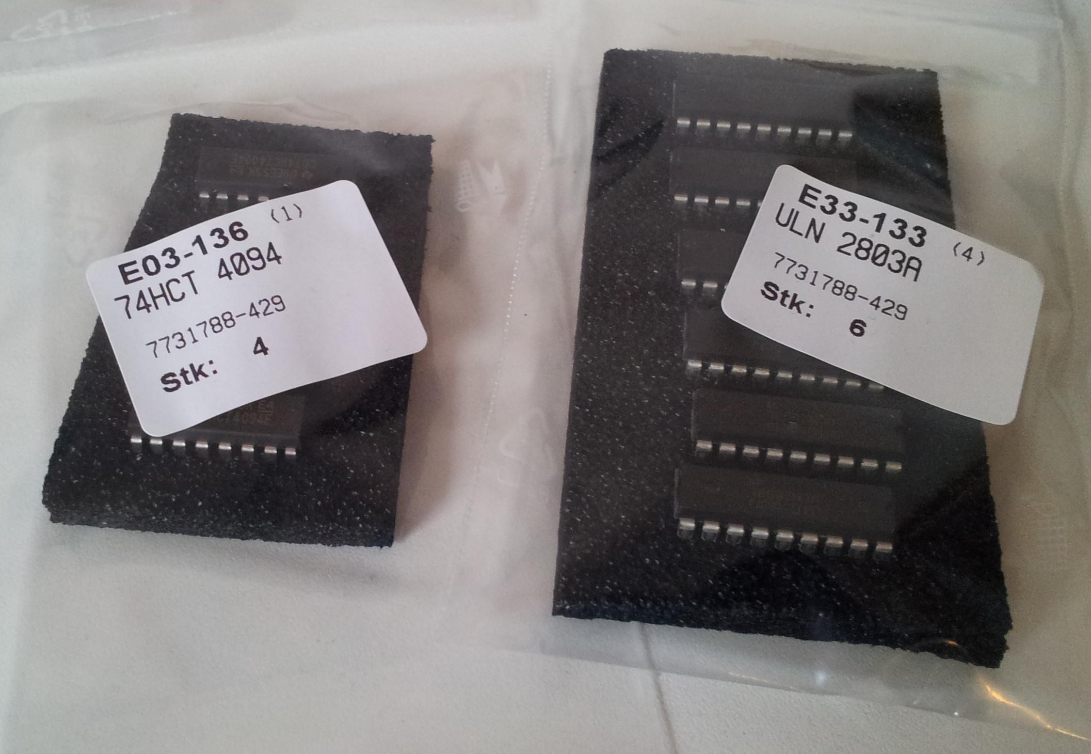
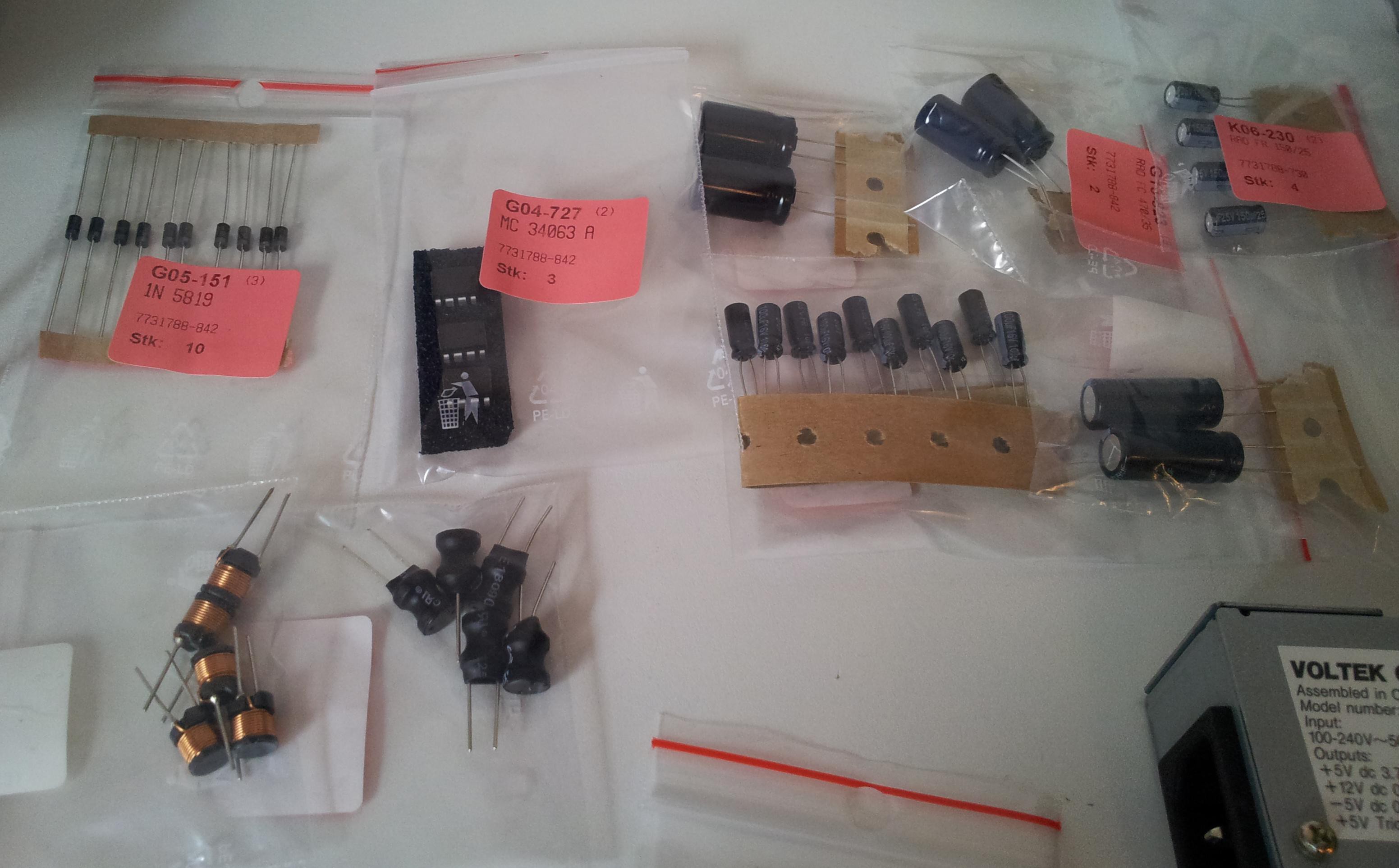
The parts have arrived
07/14/2014 at 12:58 • 0 commentsMy ordered parts arrived!
Some ink cartridges with integrated print head:
![]()
Shift register and Darlington Arrays:
![]()
Switching regulators, Schottky diodes, low ESR electrolytic capacitors, inductors:
![]()
Next thing to do: Making a concept video and then start building.
-
Added some details
07/09/2014 at 23:59 • 0 commentsOrdered missing parts, set an initial goal for August.
Digital Stamp with Inkjet Printing
Adding digital to a stamp. Print anything anywhere on any plane, inkjetable surface.