0%
0%
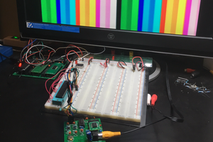
MSX2(+) video to VGA conversion (proof of concept)
V9938 and V9958 Video display processors were successors to TMS99X8 - this is an attempt to convert their video signal to VGA using FPGA
 zpekic
Become a Hackaday.io member
Already have an account? Log in.
Just one more thing
To make the experience fit your profile, pick a username and tell us what interests you.
Pick an awesome username
hackaday.io/
Your profile's URL: hackaday.io/username. Max 25 alphanumeric characters.
Pick a few interests
Projects that share your interests
People that share your interests


 JLAM
JLAM
 Peter Hizalev
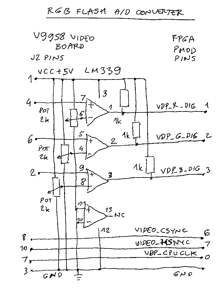
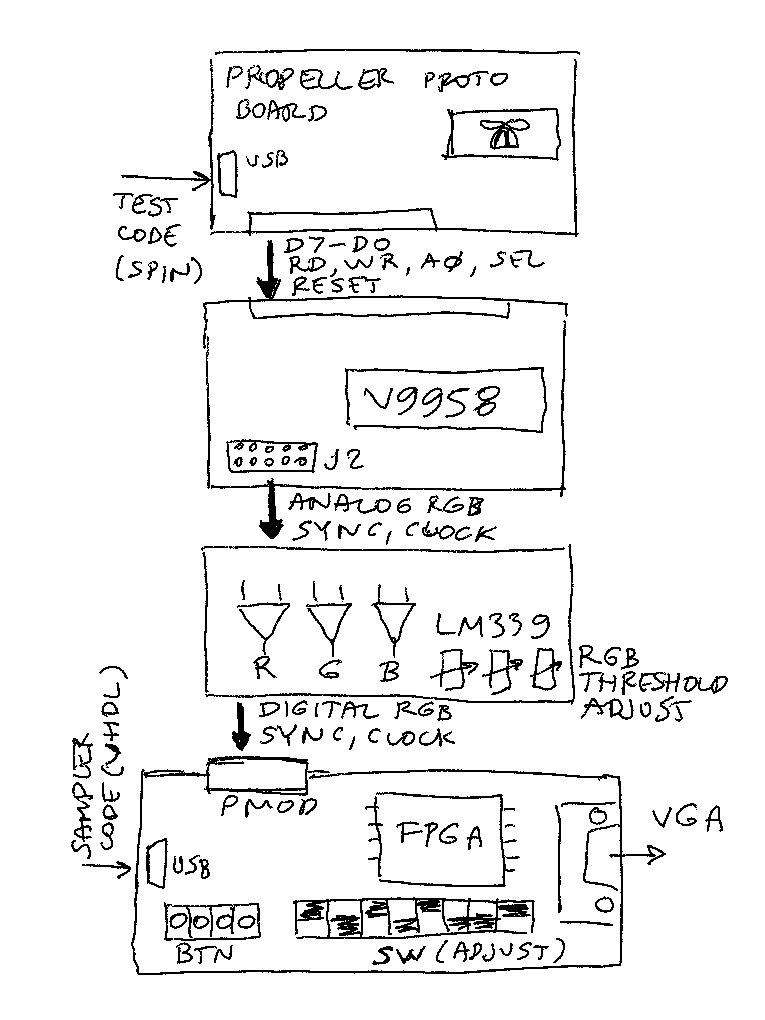
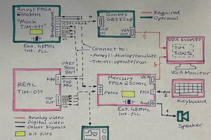
If the color bus works as expected, one could envision a V99X8 based "adapter" which could plug into TMS99X8 DIP footprint and output any number of video signals, including VGA. Although I suspect on a quality PCB with better components even a variation of my RGB flash A/D hack would work much better. Cheapest possible FPGA on such a board would be sufficient, as long as it has 32k dual RAM for the video buffer. This would be similar to famous F18A board. https://www.eetimes.com/creating-the-f18a-an-fpga-based-tms9918a-vdp/#